Optical element, optical drop module, optical add-drop module, and tunable light source

a technology of optical drop module and optical drop module, which is applied in the field of optical drop module, optical adddrop module, and tunable light source, can solve the problems of high cost, high yield, and difficult control of the thickness of the multilayer film filter layer, and achieve high resistivity, improve the high-speed response property, and the effect of high resistivity

Inactive Publication Date: 2005-01-20
SANTEC
View PDF13 Cites 26 Cited by
  • Summary
  • Abstract
  • Description
  • Claims
  • Application Information

AI Technical Summary

Benefits of technology

[0031] Moreover, in the present invention, a conductive buffer layer is formed between at least one of the first composite stack layer and the second composite stack layer and the spacer layer. In other words, the conductive buffer layer may be present on the face of the spacer layer, or may be present on both of the faces thereof. The introduction of the conductive buffer layer allows high-speed response and also allows epitaxial growth of an electrooptical film to easily take place. For this purpose, the conductive buffer layer may be formed on only the base conductive layer. This case is advantageous in that an increase in the insertion loss at the time of varying a wavelength is cut to half.
[0032] In the case where the conductive film has high resistivity and its resistance value consequently limits the high-speed responding property, the formation of the conductive buffer layer in contact with the spacer layer makes it possible to improve the high-speed responding property.
[0033] As described above, in accordance with the present invention, by altering the film design, it is possible to realize an optical element having an optional passband width and a signal eliminating characteristic for signals with the other wavelengths. Since the wavelength is changed by controlling the refractive index, no mechanical driving units are required, making it possible to improve reliability. The optical element is also excellent in environment resistance. Moreover, by designing films, the optical element of the present invention can achieve a tunable optical filter having an optional passband width and a signal eliminating characteristic for signals with other wavelengths, that is, various filters such as a lowpass filter, highpass filter, bandpass filter and notch filter. The present invention simply requires electrode terminals and circuit components to be used for controlling an applied voltage so that it is possible to form a tunable optical filter at low cost.
[0034] Moreover, by utilizing a wavelength selection unit that controls a voltage to be applied to the first and second conductive films in each of the cavities, it is possible to realize an optical drop module and an optical add-drop module having an optional passband width and a signal eliminating characteristic for signals with other wavelengths. The present invention simply requires electrode terminals and circuit components to be used for controlling an applied voltage so that it is possible to form a tunable light source at low cost.

Problems solved by technology

This is because, as the number of cavities increases to double, triple and so on, the film thickness control of each layer which constitutes the multilayer film filter becomes difficult.
Moreover, it is difficult to produce the filters with high yield, causing very high costs.
Therefore, even in an attempt to apply the tunable optical filter 101 to this OADM, there is a limitation in the response speed upon changing the wavelength to be added or dropped.
For this reason, although it is possible to meet a limited request such as a request for assigning a specific communication path to a specific customer during a predetermined time zone, it is impossible to dynamically select a wavelength to be added or dropped at a high speed.
However, since the tunable optical filter 114 uses mechanisms such as the DC motor 123 and the reduction gear 122, such mechanisms limits a high-speed response.
Therefore, the application to the optical measuring field requiring a high-speed tunable function, such as spectroscopic analysis, remote sensing, gas analysis, optical memory and optical medical diagnosis, is limited.
Moreover, the filter properties are more susceptible to environmental influences such as humidity and temperature.
For this reason, it becomes difficult to obtain superior properties with respect to incident light with a high output.
An attempt to carry out a DC driving operation would cause a dielectric breakdown.
The resulting problem is that, although the tunable optical filter 131 is allowed to change the wavelength, it fails to maintain the wavelength in a fixed state within a desired filter wavelength.
Moreover, a optical add-drop module, optical drop module, and tunable light source using the abovementioned tunable optical filters have the same problems.

Method used


Image

  • Optical element, optical drop module, optical add-drop module, and tunable light source
  • Optical element, optical drop module, optical add-drop module, and tunable light source
  • Optical element, optical drop module, optical add-drop module, and tunable light source

Examples


first embodiment

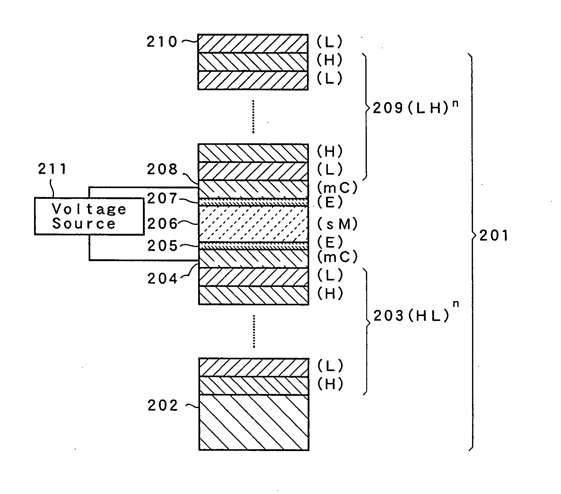
[0092] The following description will discuss embodiments of the present invention. FIG. 8 shows a schematic cross-sectional structure of an optical element in accordance with a first embodiment of the present invention. This optical element 201 has a structure in that a first mirror stack layer 203 is formed on a substrate 202 with a first conductive thin film 204 being formed thereon. The first mirror stack layer 203 and the first conductive thin film 204 constitute a first composite stack layer. Then, a conductive buffer layer 205 is formed thereon, and a spacer layer 206, which is a dielectric thin film that exerts a primary electrooptic effect or a secondary electrooptic effect, and a conductive buffer layer 207 are further formed thereon. Moreover, a second composite stack layer, constituted by a second transparent conductive film 208 and a second mirror stack layer 209, is formed thereon. A coupling layer 210 is formed on the second mirror stack layer 209. The first transpare...

second embodiment

[0147] The following description will discuss an embodiment in which the above-mentioned optical element is practically applied to a bandpass filter, in detail. FIG. 10 shows a structure of a single cavity-type tunable bandpass filter in accordance with a second embodiment of the present invention. This single cavity-type tunable bandpass filter 301 of the present embodiment has a structure in that a first mirror stack layer 303 is formed on a substrate 302; a first transparent conductive film 304, a conductive buffer layer 305, a spacer layer 306, a conductive buffer layer 307 and a second transparent conductive film 308 are stacked thereon in succession; and a second mirror stack layer 309 is further placed thereon. A coupling layer 310 is placed on the second mirror stack layer 309. Holes 321 and 322, which reach the first transparent conductive film 304 and the second transparent conductive film 308 are formed through ion milling processes, etching processes and the like. A firs...

third embodiment

[0184]FIG. 19 shows an appearance of a double cavity-type tunable bandpass filter in accordance with the third embodiment of the present invention. This double cavity-type tunable bandpass filter 401 has a structure in that a first cavity 403 is formed on a glass substrate 402 made of MgO single crystal having a refractive index of 1.72 and a second cavity 404 is formed thereon. A coupling layer 405 is placed as the uppermost layer of the second cavity 404. First to fourth holes 4061 to 4064, each having a depth reaching an electrode (not shown) on respective layer, are formed in the surface of the coupling layer 405. One end of each of wires 4071 and 4072 for the first cavity is inserted to each of the first and second holes 4061 and 4062, and bonded to an electrode, not shown. The other end of each of the wires 4071 and 4072 for the first cavity is connected to a first voltage source 4081 for the first cavity 403. Moreover, one end of each of wires 4073 and 4074 for the second cav...


PUM

PropertyMeasurementUnit
thicknessaaaaaaaaaa
resistivityaaaaaaaaaa
thicknessaaaaaaaaaa

Abstract

An optical element has a structure in that a first mirror stack layer is formed on a substrate. A first transparent conductive film, a conductive buffer layer, a spacer layer having a primary or secondary electrooptic effect, a conductive buffer layer and a second transparent conductive film are stacked thereon in succession; and a second mirror stack layer is further formed thereon. A voltage is applied between the first and second transparent conductive films. The applied voltage change the refractive index of the spacer, changes a wavelength to be transmitted through or reflected from the layer.

Description

BACKGROUND OF THE INVENTION [0001] 1. Field of the Invention [0002] The present invention relates to an optical element, an optical drop module, an optical add-drop module, and a tunable light source, using such an optical element. [0003] 2. Discussion of the Related Art [0004] Optical bandpass filters have been used for selecting light with a specific wavelength from inputted light rays. Among the bandpass filers, a tunable optical filter capable of changing a wavelength to be selected is applied various cases. For example, the tunable filter is used as a component of a multi-channel analyzer so as to change the wavelength to measure properties of a substance. The typical application has been proposed in JP-A 08-227014 (1996). This tunable optical filter has realized tunable characteristic by changing the physical film thickness. [0005]FIG. 1 shows a tunable optical filter in accordance with a first prior art. This tunable optical filter 101 has a structure in that a dielectric mul...

Claims


Application Information

Patent Timeline
Patent Type & Authority Applications(United States)
IPC IPC(8): G02B5/28G02B1/10G02F1/03G02F1/07
CPCG02F1/0305G02F1/21G02F2203/055
Inventor UEHARA, NOBORU
Owner SANTEC
Why Eureka
Try Eureka