

Gas barrier film
- Summary
- Abstract
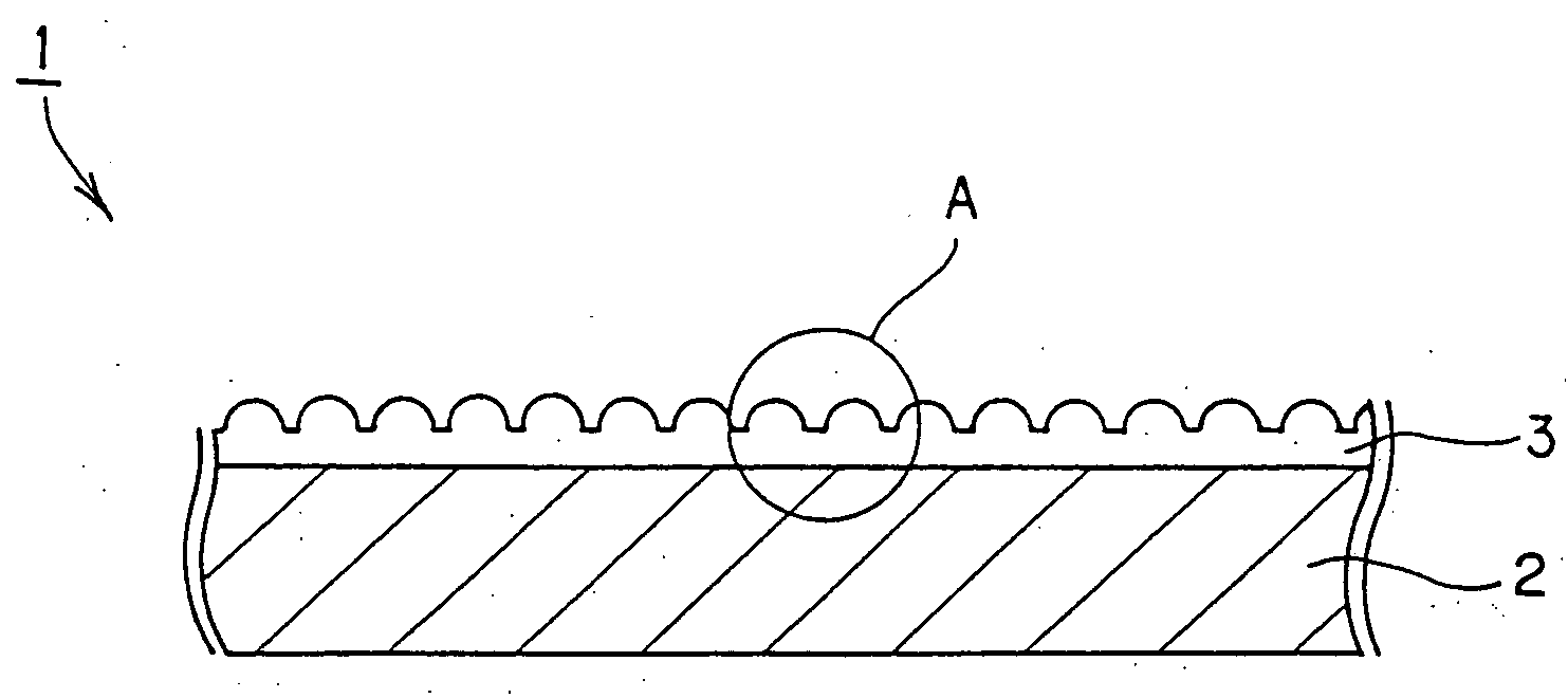
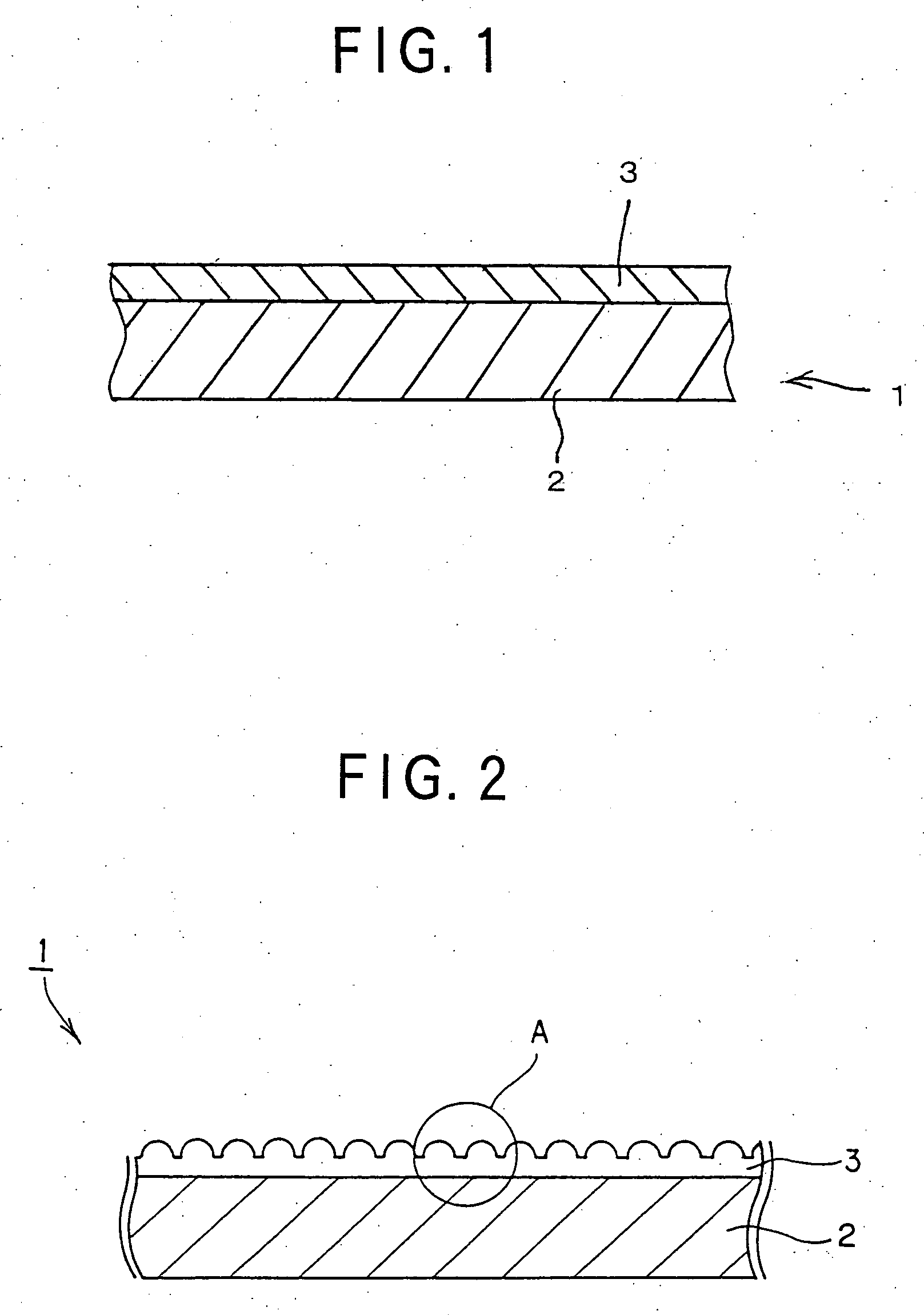
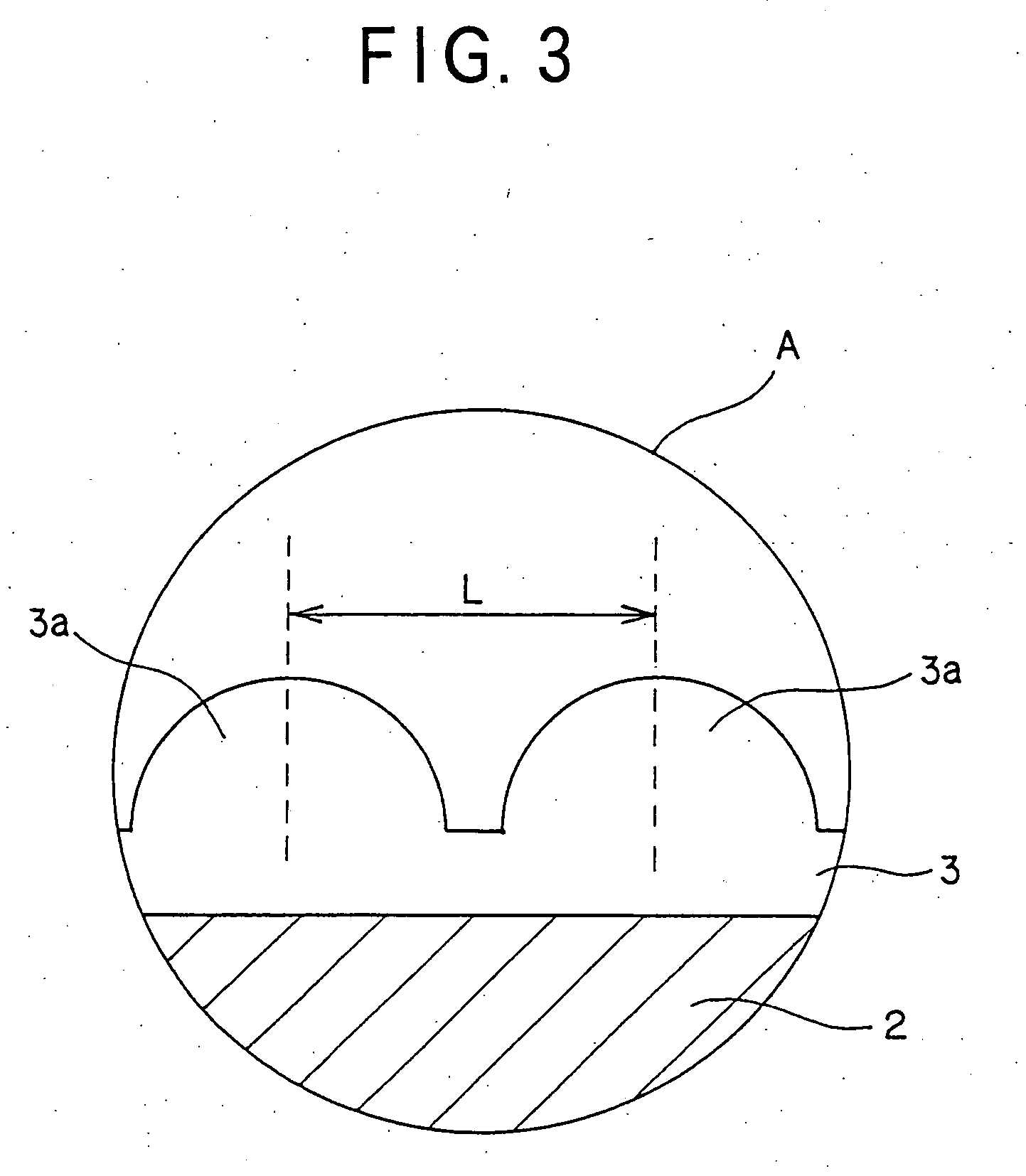
- Description
- Claims
- Application Information
AI Technical Summary
Benefits of technology
Problems solved by technology
Method used
Image

Examples
fifth embodiment
1. Fifth Embodiment
(Laminated Material)
FIG. 4 is a schematic sectional view showing the fifth embodiment of the present invention. In FIG. 4, a laminated material 11 is fitted with a gas barrier film 1 which has a vapor deposition layer 3 on the one side of a base material 2 and with a heat sealable resin layer 13 which is formed on the vapor deposition layer 3 of this gas barrier film 1 through the intermediary of an anchor coating agent layer and / or an adhesive layer 12.
The anchor coating agent layer 12 composing the laminated material 11 can be formed using, for example, organotitanic anchor coating agents such as alkyl titanate and others, isocyanate anchor coating agents, polyethylene imine anchor coating agents, polybutadiene anchor coating agents, and others. The formation of the anchor coating agent layer 12 can be made by coating an anchor coating agent as mentioned above with such a known method as, for example, roll coating, gravure coating, knife coating, dip coating...
sixth embodiment
2. Sixth Embodiment
(Laminated Material)
The sixth embodiment in the present invention is a laminated material that is characterized by a conductive layer formed on the surface of at least one side of the above-mentioned gas barrier film. FIG. 10 shows an example of the present embodiment. A laminated material in the present embodiment is made by forming conductive layer 41 on a gas barrier film 1 that is comprised of abase material 2 and a vapor deposition film (a silicon oxide film) 3 formed on the base material 2, but as shown in FIG. 10, an anchor coating layer 42 may be formed between the vapor deposition 3 and the base material 2 to improve adhesion of the vapor deposition film 3. And an overcoat layer 43 may be formed on the vapor deposition layer 3.
A gas barrier film 1 used in the present embodiment is the same as the above-mentioned gas barrier film. So the description is omitted in here.
As the conductive layer 41 used in the present embodiment, for example, an ITO fil...
examples
Though the present invention will be more concretely described by showing examples and comparative examples in the following, in gas barrier films of the present invention, there are four embodiments as a vapor deposition film formed on a base material as mentioned above. In the following, each of the embodiments will be described by citing examples and comparative examples.
PUM
| Property | Measurement | Unit |
|---|---|---|
| Temperature | aaaaa | aaaaa |
| Temperature | aaaaa | aaaaa |
| Temperature | aaaaa | aaaaa |
Abstract
Description
Claims
Application Information