

Method of forming a p-type group II-VI semiconductor crystal layer on a substrate
a technology of semiconductor crystal layer and iivi, which is applied in the direction of polycrystalline material growth, crystal growth process, chemically reactive gas, etc., can solve the problems of insufficient applicability, slow growth of p-type zno films necessary to build many electrical devices requiring p-n junctions, and inability to meet the requirements of p-type zno films, etc., to achieve the effect of lds and leds, and the resistance of these films
- Summary
- Abstract
- Description
- Claims
- Application Information
AI Technical Summary
Benefits of technology
Problems solved by technology
Method used
Image

Examples
example 1
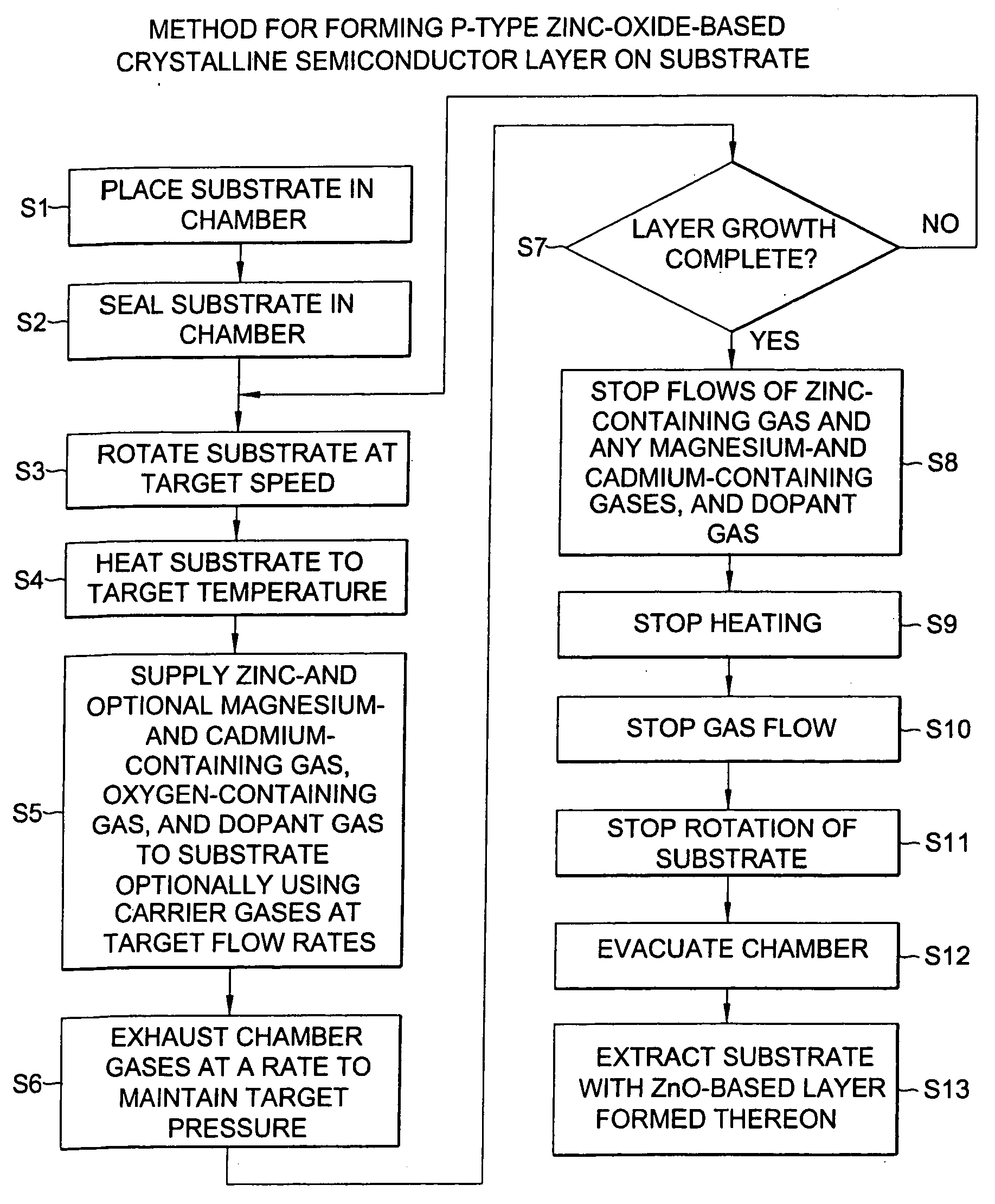
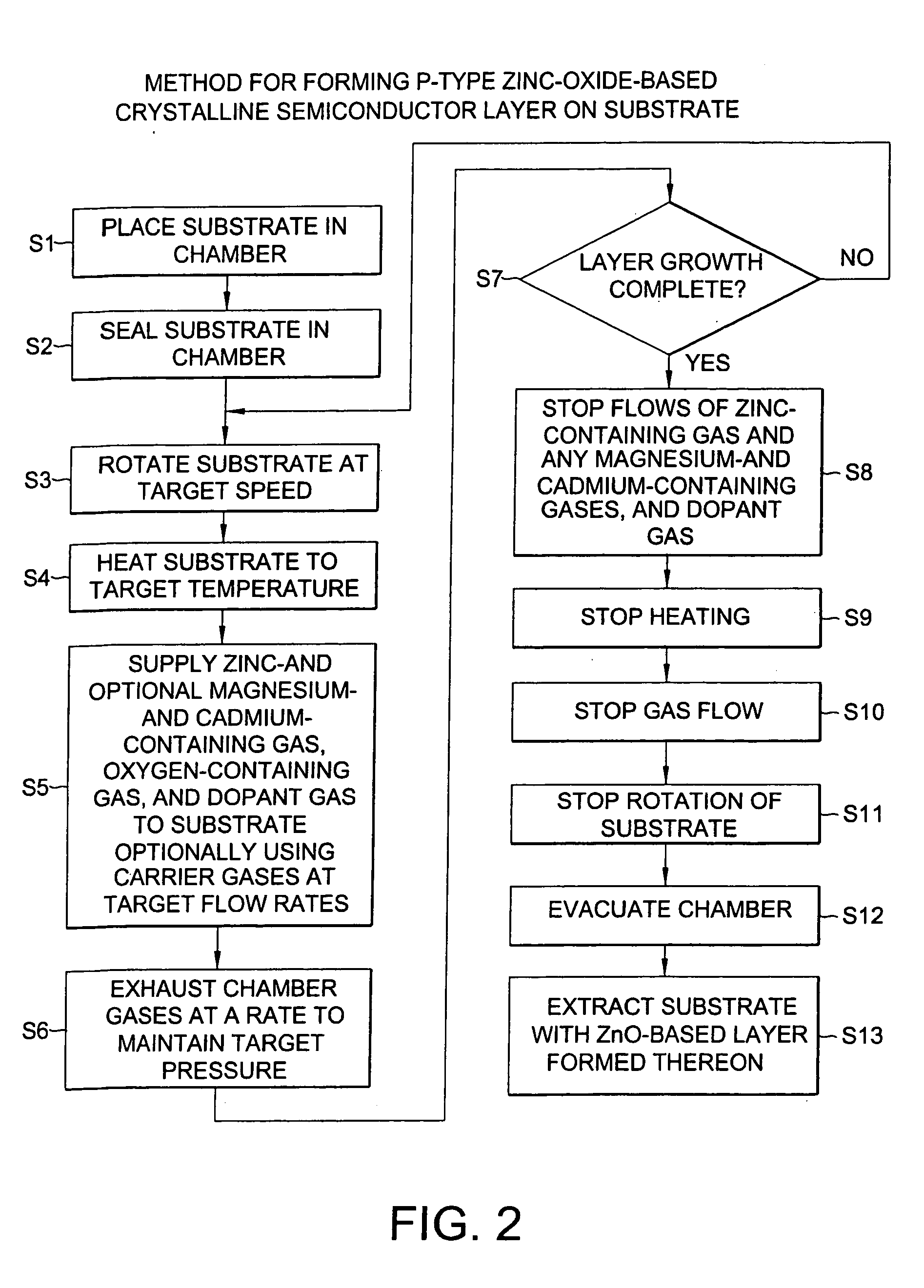
[0040] A p-type ZnO layer was grown on a ZnO substrate by the following steps.
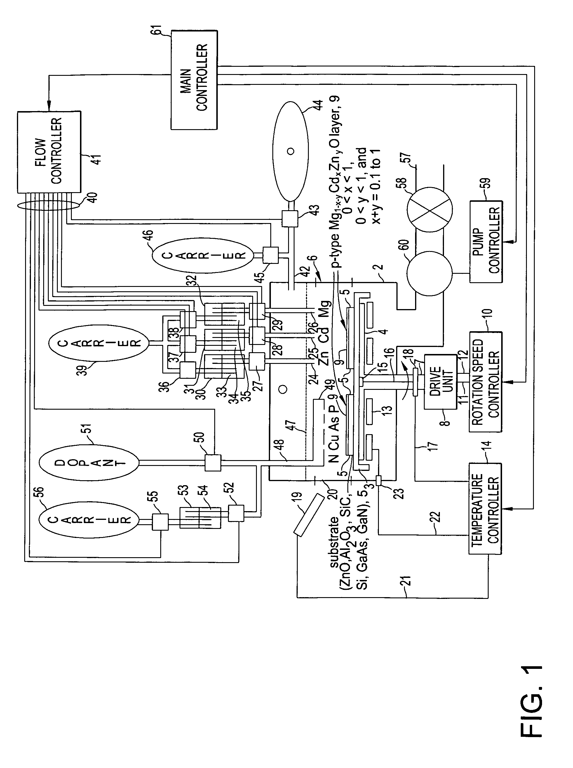
[0041] 1. Chemically cleaned, n-type ZnO single crystal substrates 5 of (002) crystallographic orientation were placed on the substrate carrier plate 3. This was then loaded onto the reactor susceptor 4 through port 6 and the chamber 2 sealed.
[0042] 2. The chamber 2 was evacuated using the exhaust pump 58 to less than one-tenth (0.1) torr pressure.
[0043] 3. A flow of three-thousand (3000) sccm argon and three-hundred (300) sccm oxygen was introduced into the chamber 2 through injection tube 42 via controllers 41, 43, 45, and tanks 44, 46 and the chamber pressure regulated to ten (10) torr with pump 58.
[0044] 4. Meanwhile, the substrate susceptor temperature was increased to four-hundred (400) degree C. and rotation rate increased to six-hundred (600) revolutions per minute (rpm) in a period of sixty (60) minutes.
[0045] 5. This state was maintained a period of time until the temperature of the suscepto...
example 2
[0054] MgZnO alloy films were grown on ZnO substrates by the following steps. [0055] 1. Chemically cleaned, n-type ZnO single crystal substrates 5 of (002) crystallographic orientation were placed on the substrate carrier plate 3. This was then loaded onto the reactor susceptor 4 and the chamber 2 sealed. [0056] 2. The chamber 2 was evacuated using the exhaust pump 58 to less than one-tenth (0.1) torr pressure.3. A flow of three-thousand (3000) sccm argon and three-hundred (300) sccm oxygen was introduced into the chamber 2 through injection tube 42 via controllers 41, 43, 45, and tanks 44, 46 and the chamber pressure regulated to ten (10) torr with pump 58.4. Meanwhile, the substrate susceptor temperature was increased to four-hundred (400) degree C. using heater 13, temperature sensor 15 or 19, and temperature controller 14, and rotation rate increased to six-hundred (600) rpm in a period of sixty (60) minutes. This state was maintained a period of time until the temperature of th...
PUM
| Property | Measurement | Unit |
|---|---|---|
| Temperature | aaaaa | aaaaa |
| Pressure | aaaaa | aaaaa |
| Temperature | aaaaa | aaaaa |
Abstract
Description
Claims
Application Information