Plasma processing system and cleaning method for the same

a technology of plasma processing and cleaning method, which is applied in the field of plasma processing system, can solve the problems of limited deposition precision, difficult to employ plasma processing system for fabricating highly precise electronic devices such as liquid crystal displays or amorphous solar batteries, and film defects in deposited films, etc., to achieve simple structure, improve the quality of deposited films, and eliminate waste.

Inactive Publication Date: 2005-02-03
SHARP KK
View PDF7 Cites 27 Cited by
  • Summary
  • Abstract
  • Description
  • Claims
  • Application Information

AI Technical Summary

Benefits of technology

[0064] As a result, since the plasma used for depositing a film is generated by the composite electrode, the quality of the deposited film can be improved by eliminating ion impact against the target substrate. In addition, since there is no need to additionally provide a cleaning electrode, products such as particles produced within the processing chamber can be efficiently removed with a simple structure, so as to improve the productivity and lower the system cost.
[0065] Furthermore, according to the present invention, a film can be deposited w

Problems solved by technology

In the conventional parallel plate type plasma processing system, however, there is a limit in the precision in the deposition due to its structure, and therefore, it is difficult to employ this plasma processing system for fabricating a highly precise electronic device such as a liquid crystal display or an amorphous solar battery.
The parallel plate type plasma processing system and the composite electrode type plasma processing system have, however, a problem that there is a fear of a film defect caused in a deposited film.
Specifically, the plasma is unavoidably spread to some extent within the processing chamber during the deposition, and therefore, unwanted films are unavoidably deposited on portions other than the target substrate such as the inner walls of the processing chamber.
Such unwanted films have comparatively low adhesion, and when their thicknesses are increased through repeated deposition, they are peeled off to form flakes, which become sources of particles.
Such particles are incorporated into the film to be deposited on the target substrate and thus cause a film defect.
In the convent

Method used


Image

  • Plasma processing system and cleaning method for the same
  • Plasma processing system and cleaning method for the same
  • Plasma processing system and cleaning method for the same

Examples


embodiment 1

[0097] Embodiment 1

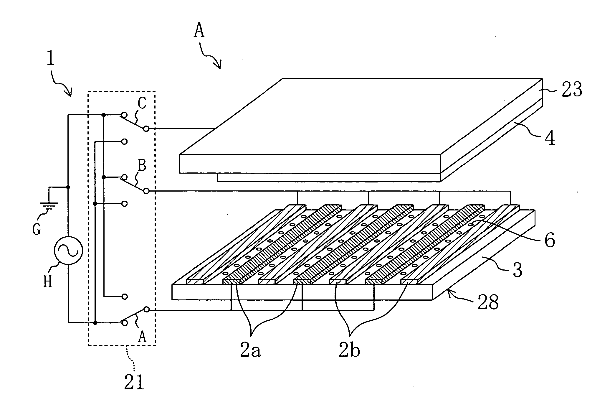
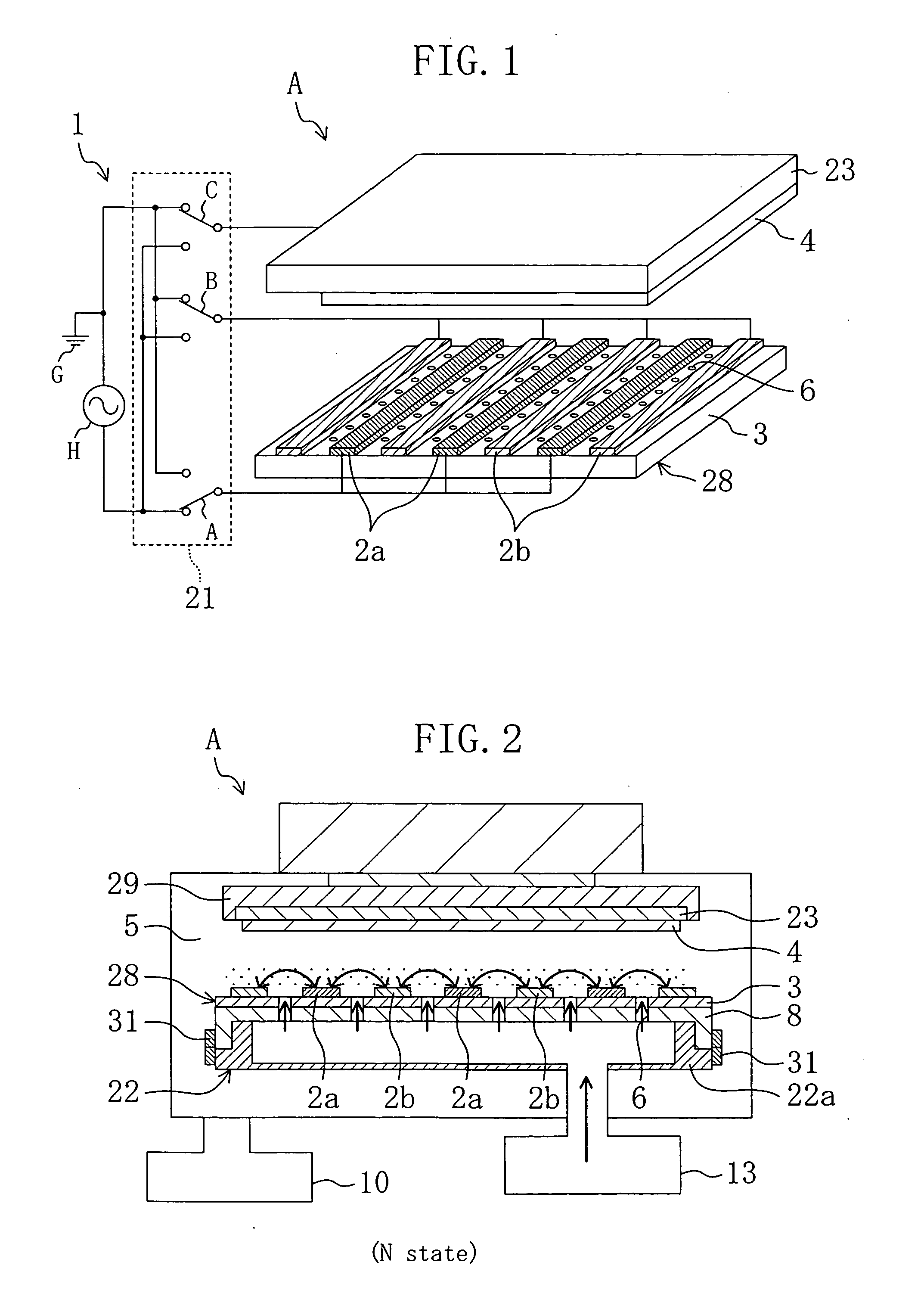
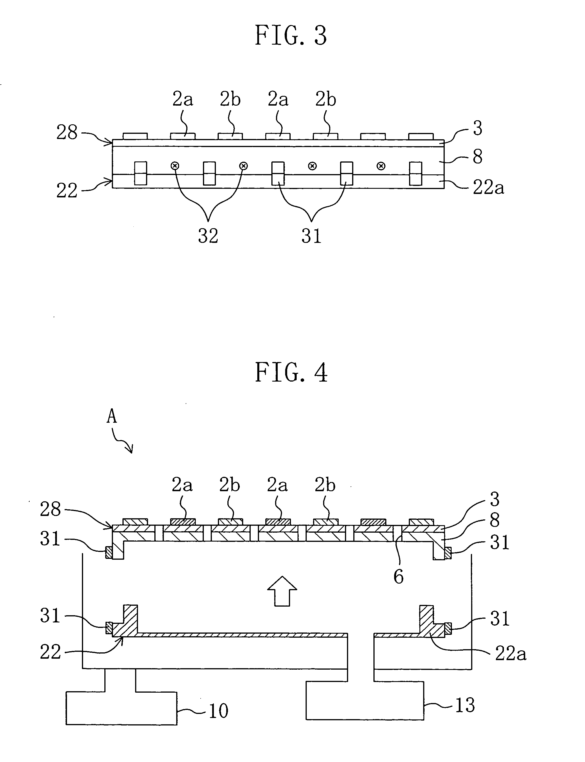
[0098]FIGS. 1 through 7 show a plasma processing system according to Embodiment 1. FIG. 1 is a schematic perspective view of a principal part of the plasma processing system and FIG. 2 is a cross-sectional view thereof.

[0099] The plasma processing system A includes, as shown in FIG. 2, a processing chamber 5, a substrate holder 23 for holding a target substrate 4 to be processed, a composite electrode 28 for generating plasma, a power circuit unit 1 and a gas supply unit 13 working as material gas supply means. Thus, the plasma processing system A is constructed as a composite electrode type plasma processing system. The target substrate 4 is subjected to plasma processing such as deposition by the plasma CVD within the processing chamber 5, and the inside of the processing chamber 5 is plasma cleaned.

[0100] The processing chamber 5 is constructed as a vacuum vessel having a door (not shown) through which the target substrate 4 is taken in / out. The processing ch...

embodiment 2

[0133] Embodiment 2

[0134]FIGS. 8 and 9 show Embodiment 2 of the present invention. It is noted that like reference numerals are used, in this and each embodiment described below, to refer to like elements shown in FIGS. 1 through 7 so as to omit the detailed description.

[0135] While the discharge state is kept to the W state in the cleaning operation in Embodiment 1, the discharge state is alternately changed between the W state and the N state during the cleaning operation in this embodiment. In other words, the switching device 21 of this embodiment switches the voltage applied state alternately between the first voltage applied state and the second voltage applied state during the cleaning operation.

[0136] Furthermore, in this embodiment, the cleaning means plasma cleans the inside of the processing chamber by using plasma generated in the plasma region increased or reduced by the plasma region increasing / reducing means 21.

[0137] The depositing operation is performed in the sa...

embodiment 3

[0143] Embodiment 3

[0144]FIG. 10 shows Embodiment 3 of the present invention. While the discharge state is kept to the W state in the cleaning operation in Embodiment 1, the discharge state is kept to the W state or the N state and a period for keeping the N state is longer than a period for keeping the W state in the cleaning operation in this embodiment. In other words, in the cleaning operation, the switching device 21 of this embodiment switches the voltage applied state so that a period for keeping the first voltage applied state can be longer than a period for keeping the second voltage applied state.

[0145] The cleaning means performs the plasma cleaning of the inside of the processing chamber 5 by using plasma generated in the plasma region increased or reduced by the plasma region increasing / reducing means corresponding to the switching device 21.

[0146] In the case where the plasma processing system A is subjected to the cleaning, the switch B is switched as shown in FIG. ...


PUM

PropertyMeasurementUnit
Frequencyaaaaaaaaaa
Frequencyaaaaaaaaaa
Pressureaaaaaaaaaa

Abstract

A plasma processing system includes a processing chamber, a substrate holder provided within the processing chamber for holding a target substrate, a composite electrode provided within the processing chamber so as to oppose the substrate holder and having a plurality of first electrodes and second electrodes for generating plasma, and a gas supply section for supplying a material gas into the processing chamber. The system further includes a plasma region increasing/reducing section for increasing or reducing a plasma region formed in the processing chamber, and a cleaning section for plasma cleaning the inside of the processing chamber by using plasma generated in the plasma region increased or reduced by the plasma region increasing/reducing section. Thus, the quality of a film to be deposited can be improved by eliminating ion impact against the target substrate, and the system cost can be lowered by efficiently removing, with a simple structure, particles produced in the processing chamber.

Description

CROSS REFERENCE TO RELATED APPLICATIONS [0001] This Nonprovisional application claims priority under 35 U.S.C. §119(a) on Patent Application No. 2003-283083 filed in Japan on Jul. 30, 2003 and Patent Application No. 2004-171598 filed in Japan on Jun. 9, 2004, the entire contents of which are hereby incorporated by reference. BACKGROUND OF THE INVENTION [0002] The present invention relates to a plasma processing system that performs, in a processing chamber, plasma processing by plasma-activated chemical vapor deposition, dry etching, ashing and the like and cleans the inside of the processing chamber with plasma, and a plasma cleaning method for the system. [0003] The plasma-activated chemical vapor deposition (hereinafter referred to as the plasma CVD) for depositing a semiconductor film or the like by using plasma is conventionally known. A conventional parallel plate type plasma processing system for depositing a film on a target substrate by the plasma CVD will be described with...

Claims


Application Information

Patent Timeline
IPC IPC(8): H05H1/46C23C16/00C23C16/44C23C16/509H01L21/00H01L21/205H01L21/302H01L21/3065
CPCC23C16/4405H01J37/32862C23C16/5096H01L21/205H01L21/302
Inventor HATANO, AKITSUGU
Owner SHARP KK
Why Eureka
Try Eureka