Atomic layer deposition of metal oxide and/or low asymmetrical tunnel barrier interpoly insulators

a tunnel barrier and metal oxide technology, applied in the field of integrated circuits, can solve the problems of premature breakdown and reliability problems, poor quality of interpoly oxides, and localized high electric fields

Inactive Publication Date: 2005-02-03
MICRON TECH INC
View PDF99 Cites 337 Cited by
  • Summary
  • Abstract
  • Description
  • Claims
  • Application Information

AI Technical Summary

Benefits of technology

The above mentioned problems with programmable array type logic and/or memory devices and other problems are addressed by the present invention and will be understood by reading and st

Problems solved by technology

However, the rough top surface of the polysilicon floating gate resulted in, poor quality interpoly oxides, sharp points, localized high electric fields, premature breakdown and reliability problems.
However, in order to enable a reasonable write speed the ETOX cell uses channel hot electron injection, the erase operation which can be slower is achieved by Fowler-Nordhiem tunneling from the floating gate to the source.
The large barriers to electron tunneling or hot electron injection presented by the silicon oxide-silicon interface, 3.2 eV, result in slow write and erase speeds even at very high electric fields.
The combination of very high electric fields and damage by hot electron collisions in the oxide result in a number of operational

Method used


Image

  • Atomic layer deposition of metal oxide and/or low asymmetrical tunnel barrier interpoly insulators
  • Atomic layer deposition of metal oxide and/or low asymmetrical tunnel barrier interpoly insulators
  • Atomic layer deposition of metal oxide and/or low asymmetrical tunnel barrier interpoly insulators

Examples


example i

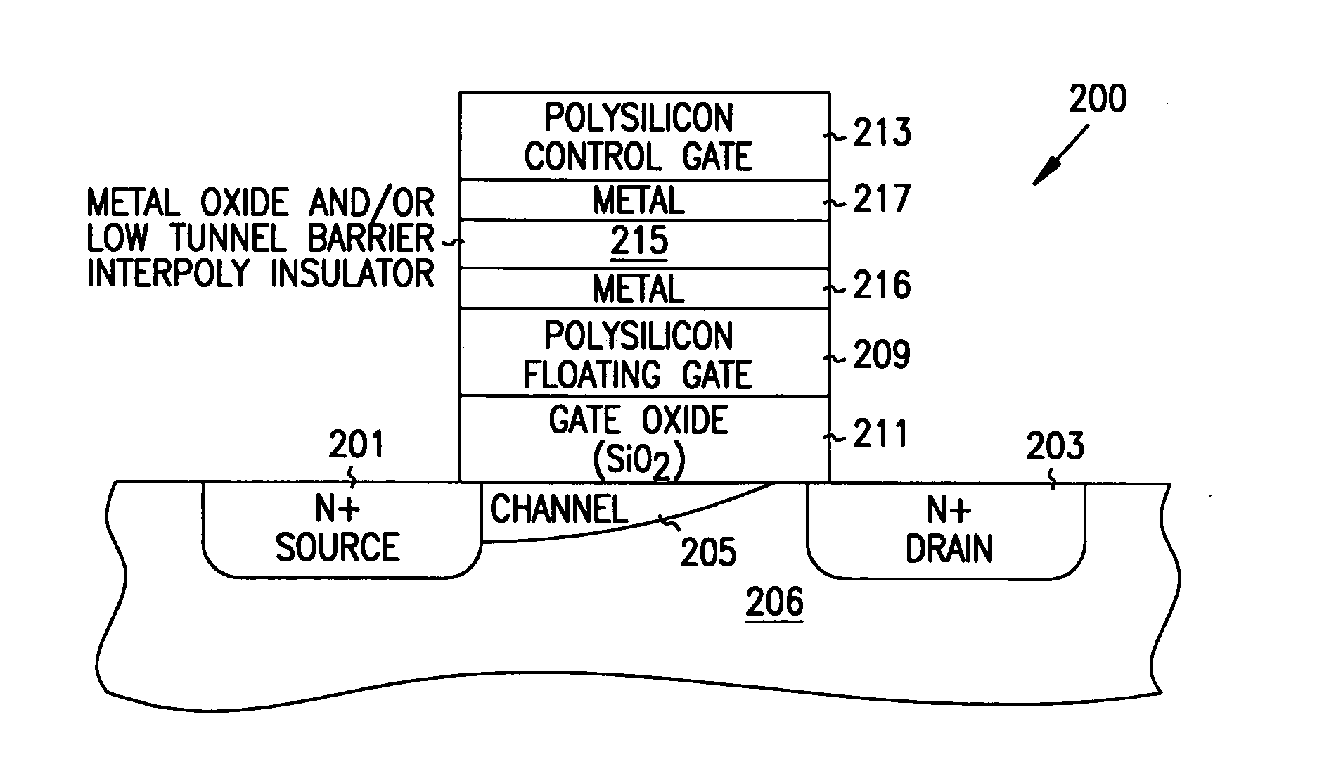
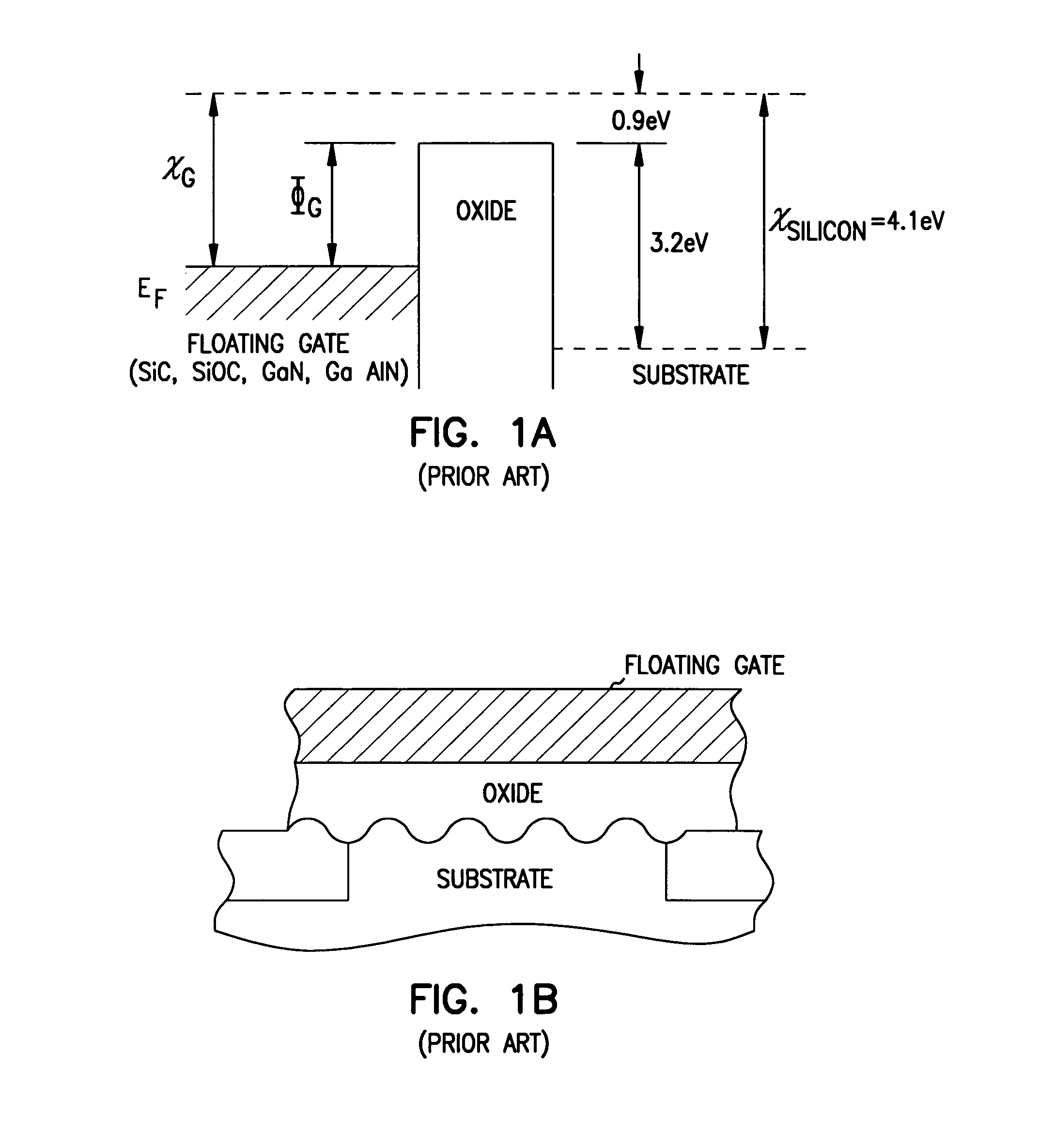
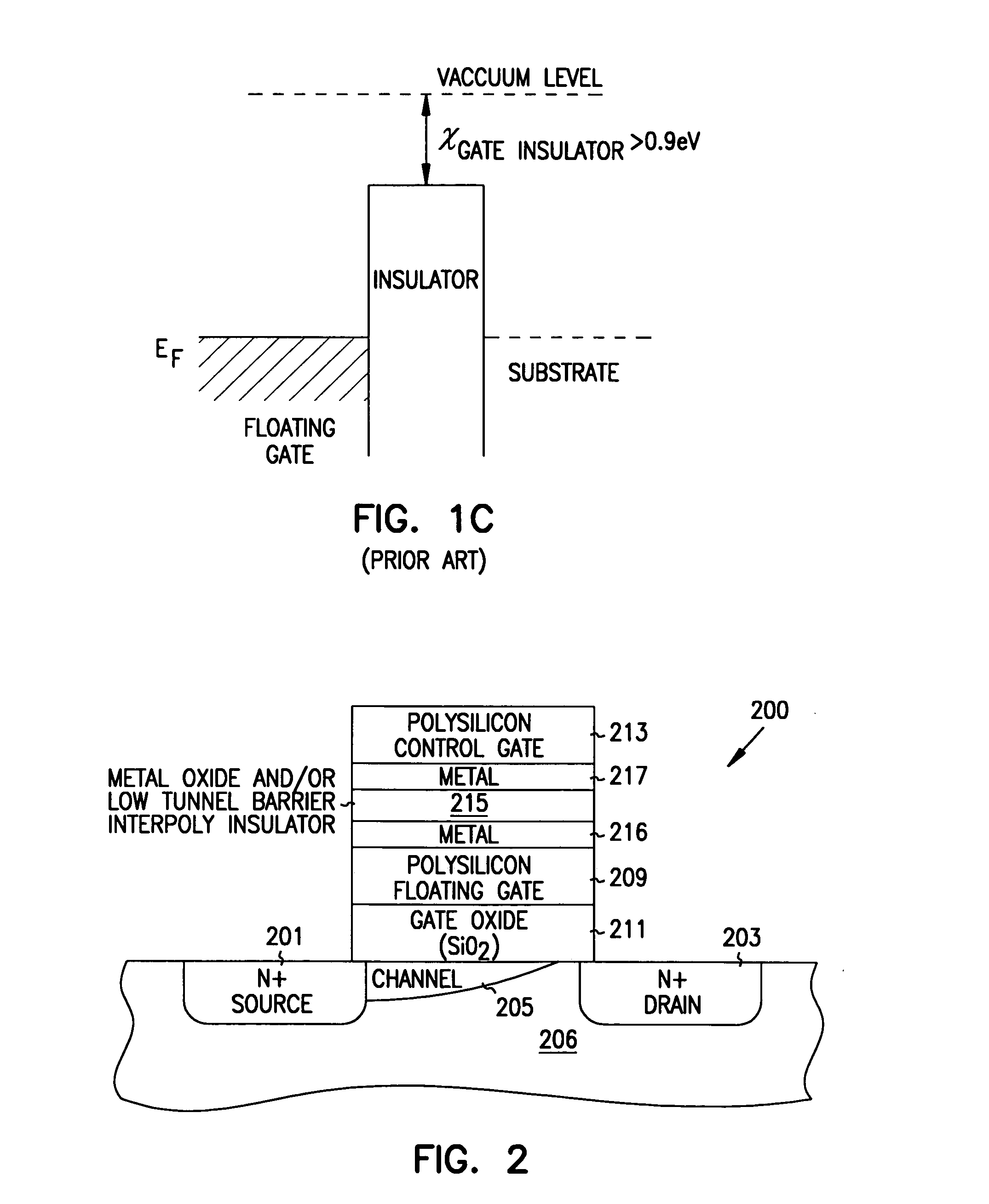
Formation of Al / Al2O3 / Al tunnel barriers can be built having a barrier height of about ˜2 eV. FIG. 8 graphically illustrates the dependence of the barrier height for current injection on the work function and electron affinity of a given, homogeneous dielectric film. FIG. 9 is a table which provides relevant data on the barrier heights, energy gaps, dielectric constants and electron affinities of a wide variety of metal oxides that could be used as asymmetric tunnel barriers according to the teachings of the present invention. (See generally, H. F. Luan et al., “High quality Ta2O5 gate dielectrics with Tox equil. 10 Angstroms,” IEDM Tech. Digest, pp. 141-144, 1999; J. Robertson et al., “Schottky barrier heights of tantalum oxide, barium strontium titanate, lead titanate and strontium bismuth tantalate,” App. Phys. Lett., Vol. 74, No. 8, pp. 1168-1170, February 1999; J. Robertson, “Band offsets of wide-band-gap oxides and implications for future electronic devices,” J. Vac. Sci. Tec...

example ii

Formation of Al / Ta2O5 / Al tunnel barriers can be formed with a barrier height of about 2 eV. See FIGS. 8 and 9. Again, processes for producing ultra-thin films of Ta2O5 that are suitable for tunnel barriers are known. See, for example, the work of Kim et al. (see generally, Y. S. Kim et al., “Effect of rapid thermal annealing on the structure and the electrical properties of atomic layer deposited Ta2O5 films”, Jour. Korean Phys. Soc. 37 (6), pp. 975-979 (2000)) cited above. Note that it may not be necessary to maximize the dielectric constant of this oxide for the present applications although such maximization is desirable for building useful, minimal area DRAM storage capacitors. One can fabricate these Al / Ta2O5 / Al tunnel barriers following the approach sketched out above. (i) Use a low energy, inert ion plasma in the auxiliary chamber to sputter clean residual exodies, etc. from the poly-Si surfaces previously fabricated on the device wafer. (ii) Deposit an aluminum contact la...


PUM


Abstract

Structures and methods for programmable array type logic and/or memory devices with asymmetrical low tunnel barrier intergate insulators are provided. The programmable array type logic and/or memory devices include non-volatile memory which has a first source/drain region and a second source/drain region separated by a channel region in a substrate. A floating gate opposing the channel region and is separated therefrom by a gate oxide. A control gate opposes the floating gate. The control gate is separated from the floating gate by an asymmetrical low tunnel barrier intergate insulator formed by atomic layer deposition. The asymmetrical low tunnel barrier intergate insulator includes a metal oxide insulator selected from the group consisting of Al2O3, Ta2O5, TiO2, ZrO2, Nb2O5, SrBi2Ta2O3, SrTiO3, PbTiO3, and PbZrO3.

Description

FIELD OF THE INVENTION The present invention relates generally to integrated circuits, and in particular to programmable array type logic and / or memory devices with asymmetrical low tunnel barrier interpoly insulators. BACKGROUND OF THE INVENTION Flash memories have become widely accepted in a variety of applications ranging from personal computers, to digital cameras and wireless phones. Both INTEL and AMD have separately each produced about one billion integrated circuit chips in this technology. The original EEPROM or EARPROM and flash memory devices described by Toshiba in 1984 used the interpoly dielectric insulator for erase. (See generally, F. Masuoka et al., “A new flash EEPROM cell using triple polysilicon technology,” IEEE Int. Electron Devices Meeting, San Francisco, pp. 464-67, 1984; F. Masuoka et al., “256K flash EEPROM using triple polysilicon technology,” IEEE Solid-State Circuits Conf., Philadelphia, pp. 168-169, 1985). Various combinations of silicon oxide and si...

Claims


Application Information

Patent Timeline
IPC IPC(8): G11C16/04H01L21/8247H01L27/115H01L29/51H01L29/788
CPCG11C16/0416H01L21/28273H01L27/115H01L27/11521H01L29/7885H01L29/51H01L29/511H01L29/513H01L29/66825H01L27/11556H01L29/40114H10B69/00H10B41/30H10B41/27
Inventor ELDRIDGE, JEROME M.AHN, KIE Y.FORBES, LEONARD
Owner MICRON TECH INC
Why Eureka
Try Eureka