Low-inductance circuit arrangement for power semiconductor modules

a low-inductance circuit and power semiconductor technology, applied in emergency protective arrangements, electrical apparatus contruction details, instruments, etc., can solve the problems of low parasitic inductance in this circuit arrangement, and the effect of reducing the substrate surface available, low loss, and low parasitic inductan

Inactive Publication Date: 2005-02-03
SEMIKRON ELECTRONICS GMBH & CO KG
View PDF13 Cites 48 Cited by
  • Summary
  • Abstract
  • Description
  • Claims
  • Application Information

AI Technical Summary

Benefits of technology

[0021] It is another object of the present invention to provide a circuit arrangement in which (1) the entire arrangement has low parasitic inductances, (2)the input and output current leads to the semiconductor components are of reduced ohmic inductance, and (3) in which the semiconductor components and the port conductors require only a small total surface, whereby the port conductors (alternatively connecting conductors, hook-up conductors, terminal conductors etc.) only slightly reduce the substrate surface available for the required semiconductor components.
[0022] The present invention relates to a circuit arrangement for a power semiconductor module provides low parasitic inductances and low loss. An electrically insulating substrate supports metallic ribbon connectors which in turn power attached semiconductor components. DC port conducts are positioned in close proximity to each other and are arranged in at least one partial sector parallel and in close proximity to the surface of the substrate and / or the ribbon connectors and electrically insulated from the same, and at least one AC port conductor is similarly attached. The port conductors include surface elements enabling simplified low-inductance wire bond connection from the port conductors to either the power semiconductor components or ribbon connectors or both.

Problems solved by technology

Similarly, DE 196 18 978 A1 discloses a comparable arrangement for the load ports, unfortunately, the entire arrangement including the substrate is not of sufficiently low inductance, since the current-circumfused (current surrounded) surfaces (see description in DE 100 37 533 C1) are too large.
Unfortunately, the low parasitic inductances in this circuit arrangements, achieved with this pressure-contacted arrangement, are still limited.
Unfortunately, these port conductors are auxiliary port conductors which, in contrast to the load port conductors consisting of DC and AC port conductors, have no effect on the parasitic inductances of the power semiconductor module.
Unfortunately, in EP 0 277 546, while the transistors forming the individual switch are in close proximity to each other, the current can nevertheless flow through the circuit arrangement along dissimilar paths, in particular along paths of dissimilar length.
This design results in dissimilar current-circumfused surfaces, dissimilar inductances for the different conduction paths, and also dissimilar ohmic resistance values for these conduction paths.
As a particular detriment to this design, the design of a half-bridge with such individual switches can never be of low inductance due to the external circuitry necessary for that purpose.
Unfortunately, the design shown does not meet all the requirements for minimizing parasitic inductances.
Secondly, the power transistors of the first and second power switches are relative far apart, which also increases the parasitic inductances.
In sum, the unfortunate consequence of the above-mentioned related art teachings are circuit designs having ineffective low-inductance design and result in substantially larger parasitic inductances than necessary.

Method used


Image

  • Low-inductance circuit arrangement for power semiconductor modules
  • Low-inductance circuit arrangement for power semiconductor modules
  • Low-inductance circuit arrangement for power semiconductor modules

Examples


Embodiment Construction

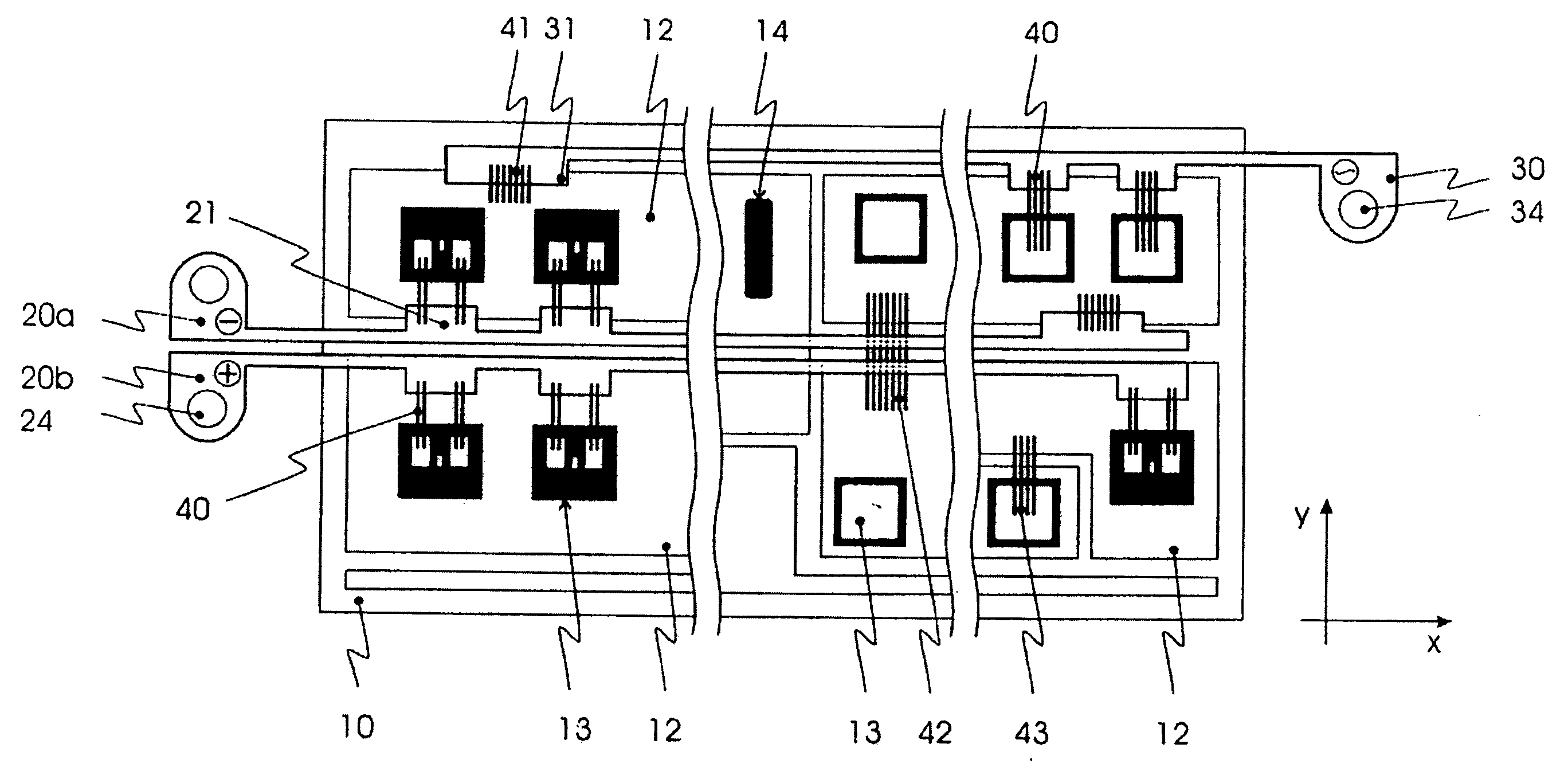
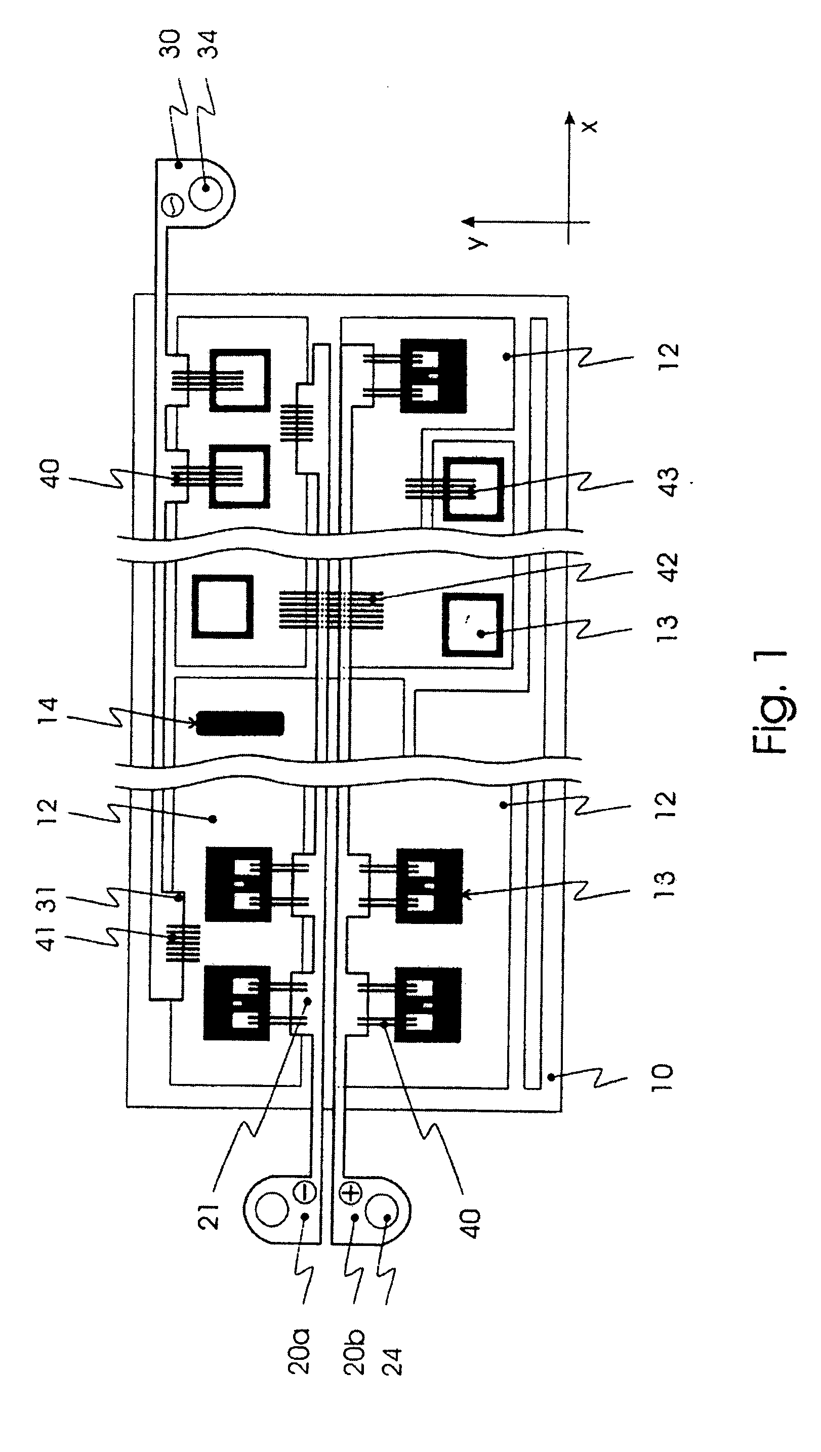
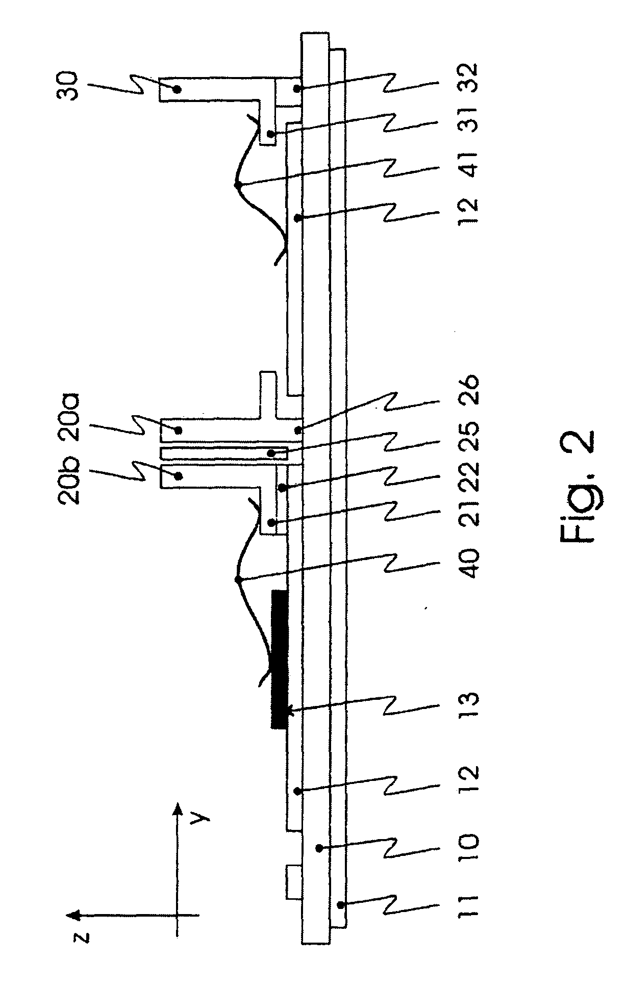
[0059] The present invention relates to a low-inductance circuit arrangement for power semiconductor modules. More specifically, the present invention relates to a low-inductance circuit arrangement for modem power semiconductor modules providing and using preferred high-speed, low-loss semiconductor switches as taught herein. The present invention similarly provides a circuit with unique design having low parasitic inductances and a compact size.

[0060] According to the present invention the present design is adapted for use with MOSFETs or insulated gate bipolar transistors (IGBTs) with free-running diodes in antiparallel type connections which are especially suited as power semiconductor components for this circuit arrangement. Such circuit arrangements and exemplary power converters designed with the same must be configured with low inductance to avoid the occurrence of debilitating or damaging voltage spikes, especially during shut-down or a breaking type current.

[0061] This m...


PUM


Abstract

A circuit arrangement for a power semiconductor module provides low parasitic inductances and low loss. An electrically insulating substrate supports metallic ribbon connectors which in turn power attached semiconductor components. DC port conducts are positioned in close proximity to each other and are arranged in at least one partial sector parallel and in close proximity to the surface of the substrate and/or the ribbon connectors and electrically insulated from the same, and at least one AC port conductor is similarly attached. The port conductors include surface elements enabling simplified low-inductance wire bond connection from the port conductors to either the power semiconductor components or ribbon connectors or both.

Description

CROSS-REFERENCE TO RELATED APPLICATIONS [0001] This application claims priority from DE 102 37 561.5, filed Aug. 16, 2002, the contents of which are incorporated fully herein by reference.SELECTED FIGURE FOR PUBLICATION [0002]FIG. 4 is selected for publication purposes. BACKGROUND OF THE INVENTION [0003] 1. Field of the Invention [0004] The present invention relates to a low-inductance circuit arrangement for power semiconductor modules. More specifically, the present invention relates to a low-inductance circuit arrangement for high-speed modem power semiconductor modules having low parasitic inductances and low ohmic resistance. [0005] 2. Description of the Related Art [0006] Power transistors such as IGBTs (Insulating-Gate Bipolar Transistors) or MOSFETs (Metal Oxide Semiconductor Field-Effect Transistors) are conventionally known. In use, power transistors such as IGBTs and MOSFETs are regulated, i.e., switched into a conductive or non-conductive state, by applying a certain vol...

Claims


Application Information

Patent Timeline
Patent Type & Authority Applications(United States)
IPC IPC(8): H01L23/12H01L25/07H01L25/18H02M7/00H02M7/04
CPCH01L24/49H01L2924/19107H01L2224/45014H01L2224/48091H01L2224/48247H01L2224/48472H01L2224/49111H01L2224/49175H01L2924/01004H01L2924/01005H01L2924/01006H01L2924/01013H01L2924/0102H01L2924/01029H01L2924/01047H01L2924/01078H01L2924/01082H01L2924/13055H01L2924/13091H01L2924/19043H01L2924/30107H02M7/003H01L25/072H01L2924/1301H01L2924/01033H01L2924/014H01L2924/1305H01L2924/00014H01L2924/00H01L2924/15787H01L2224/48137H01L2224/0603H01L2224/49113H01L24/48H01L2224/45099H01L2224/05599H01L2924/206
Inventor HEILBRONNER, HEINRICHSTOCKMEIER, THOMAS
Owner SEMIKRON ELECTRONICS GMBH & CO KG
Why Eureka
Try Eureka