Methods for reducing metal contamination on a surface of a sapphire substrate by plasma treatment

a sapphire substrate and metal contamination technology, applied in the direction of basic electric elements, electrical equipment, semiconductor devices, etc., can solve the problems of metal contamination on the substrate surface, sapphire wafer contamination, deterioration of the electrical performance of the active layer, etc., and achieve the effect of reducing metal contamination

Active Publication Date: 2017-11-07
SOITEC SA
View PDF6 Cites 0 Cited by
  • Summary
  • Abstract
  • Description
  • Claims
  • Application Information

AI Technical Summary

Benefits of technology

[0016]The present disclosure relates to a method for reducing the metal contamination on a surface of a substrate comprising a plasma treatment of the surface of the substrate by ion bombardment, wherein a plasma of a supplied gas is generated and wherein a bombardment energy of the ions in the plasma is controlled by a radio frequency electromagnetic field. The bombardment energy of the ions is higher than a first threshold to tear the metal contamination, and the bombardment energy of the ions is lower than a second threshold to prevent a surface quality degradation of the surface of the substrate.
[0017]The present disclosure aims to remove the metal contaminants on a substrate surface without degrading the surface quality, notably in terms of roughness and defectivity.
[0030]The present disclosure relates also to a bonding process to form a bond between a plasma-treated sapphire substrate surface and a semiconductor substrate surface, such as a silicon substrate, by wafer bonding, wherein the metal contamination on the sapphire substrate surface is reduced by a plasma treatment involving ion bombardment, wherein a plasma of a supplied gas is generated and wherein a bombardment energy of the ions in the plasma is controlled by a radio frequency electromagnetic field. The bombardment energy of the ions is higher than a first threshold to tear the metal contamination, and the bombardment energy of the ions is lower than a second threshold to prevent a surface quality degradation of the surface of the substrate.
[0032]The present disclosure also relates to a substrate comprising a plasma-treated sapphire substrate surface and a semiconductor substrate surface, wherein bonding is formed by wafer bonding between these two surfaces, wherein the metal contamination on the sapphire substrate surface is reduced by a plasma treatment of ion bombardment, wherein a plasma of a supplied gas is generated and wherein a bombardment energy of the ions in the plasma is controlled by a radio frequency electromagnetic field. The bombardment energy of the ions is higher than a first threshold to tear the metal contamination, and the bombardment energy of the ions is lower than a second threshold to prevent a surface quality degradation of the surface of the substrate.

Problems solved by technology

One of the challenges in semiconductor device processing is the problem of metal contamination on the substrate surface.
These metallic species are well known to deteriorate the electrical performance of the active layer.
Due to a lower manufacturing maturity, sapphire wafers can be contaminated at different steps of substrate preparation and handling processes like polishing, storage and characterization.
A large quantity of metal contamination can often be found on the surface of a sapphire substrate used for semiconductor devices.
The high temperature thermal treatments carried out during or after the fabrication process of SOS substrates trigger the migration of the metal species from the surface of the sapphire substrate toward the silicon layer, thus rendering the SOS substrates incompatible with the manufacturing of electronic devices.
Under the condition of significant iron contamination, iron silicide precipitates can form in the thin active silicon layer and degrade its electrical integrity.
However, a sapphire substrate is more chemically inert than silicon, and requires more aggressive chemical treatments for etching its surface and dissolving metallic contaminants.
This is usually why wet treatments reacting only with the surface of the substrate are not sufficiently efficient and do not meet the specific requirements for the manufacturing of electronic devices.
Additionally, for substrates with low reactivity to chemicals, such as sapphire, wet treatments are inefficient to dissolve all metal contaminant elements, even at the surface of the substrate, depending on the chemical bonds of those elements.
Chemical-mechanical polishing can eventually remove the sub-surface contaminated layer, but it remains difficult to prevent slurry contaminant residues and their slight diffusion at the close surface, and it is difficult or impossible to reach the targeted levels of residual metal contaminants.
Alternatively, a wet cleaning step based on phosphoric acid (H3PO4) chemistry and performed at high temperature (100° C. or higher) can be efficient to remove metal contamination at the surface and close sub-surface; nevertheless, this type of solution is difficult to implement in an industrial infrastructure due to safety and the degraded reliability of bath heater elements at such high temperatures.
Moreover, a residual contamination of phosphorus has been observed at the surface after such treatments, which may be unacceptable for certain targeted electronics applications given that phosphorus is a dopant for silicon.
The wet or dry chemical etch solutions currently existing are either inefficient to remove metal contamination at the surface of substrates having low reactivity (such as sapphire) or, when efficient, at least partially, they may degrade the substrate surface (local surface pitting, increased roughness, etc.) to an extent that the substrate is not suitable for further use.

Method used


Image

  • Methods for reducing metal contamination on a surface of a sapphire substrate by plasma treatment
  • Methods for reducing metal contamination on a surface of a sapphire substrate by plasma treatment

Examples


Embodiment Construction

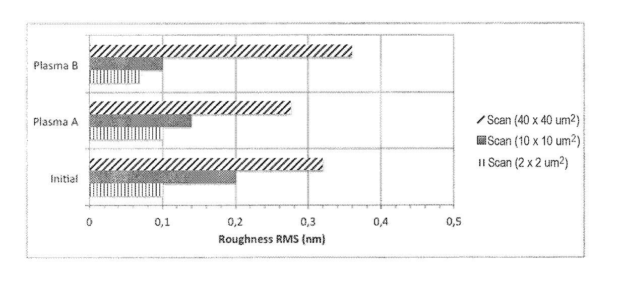
[0035]The present disclosure relates to a method for reducing the metal contamination on a surface of a substrate comprising a plasma treatment of the surface of the substrate by ion bombardment, wherein a plasma of a supplied gas is generated and wherein a bombardment energy of the ions in the plasma is controlled by a radio frequency (RF) electromagnetic field. The bombardment energy of the ions is higher than a first threshold to tear the metal contaminants from the substrate surface, and the bombardment energy of the ions is lower than a second threshold to prevent a surface quality degradation of the substrate surface.

[0036]In some embodiments, the plasma may be generated from at least one kind of noble gas. As a non-limiting embodiment, a pure noble gas, chosen among He, Ne, Ar, Kr, Xe, may be used. A mixture of different noble gases may also be used. Noble gases may be preferred relative to other gases, such as reactive gases like chlorine and boron chloride, to avoid generat...


PUM

PropertyMeasurementUnit
gas pressureaaaaaaaaaa
surface roughnessaaaaaaaaaa

Abstract

The present disclosure relates to a method for reducing metal contamination on a surface of a substrate. The method involves plasma treatment of the surface of the substrate by ion bombardment, wherein a plasma of a supplied gas is generated, and a bombardment energy of the ions in the plasma is controlled by a radio frequency electromagnetic field. The bombardment energy of the ions is higher than a first threshold so as to tear the metal contamination from the surface of the substrate, and the bombardment energy of the ions is lower than a second threshold so as to prevent a surface quality degradation of the surface of the substrate.

Description

PRIORITY CLAIM[0001]Pursuant to 35 U.S.C. §119(a), this application claims the benefit of the filing date of French Patent Application Serial No. 1552416, filed Mar. 24, 2015, for “Method for Reducing the Metal Contamination on a Surface of a Substrate,” the contents of which are incorporated herein in their entirety by this reference.TECHNICAL FIELD[0002]The present invention is related to a method for reducing the metal contamination on a surface of a substrate. Those substrates are notably used in the field of microelectronics, micromechanics, photonics and LED (light-emitting diode) devices.BACKGROUND[0003]One of the challenges in semiconductor device processing is the problem of metal contamination on the substrate surface. Semiconductor devices are extremely sensitive to minute quantities of metals present on the surface or inside the substrates. These metallic species are well known to deteriorate the electrical performance of the active layer. The silicon substrate industry ...

Claims


Application Information

Patent Timeline
Patent Type & Authority Patents(United States)
IPC IPC(8): H01L21/20H01L21/263H01L21/02H01L29/06H01L21/762H01L21/86
CPCH01L21/86H01L21/02046H01L29/0649H01L21/263H01L21/76251H01L21/2011H01L21/02315H01L21/0234H01L21/187H01L21/3065H01L21/324
Inventor BARGE, THIERRY
Owner SOITEC SA
Why Eureka
Try Eureka