Semiconductor memory device with memory cells operated by boosted voltage

a memory cell and semiconductor technology, applied in semiconductor devices, digital storage, instruments, etc., can solve the problems of high power consumption of power supply lines, inability to read, and long time for the power supply voltage vddm of memory cell arrays, etc., to achieve low power consumption, low voltage operation, and low noise margin

Inactive Publication Date: 2005-02-03
RENESAS ELECTRONICS CORP
View PDF6 Cites 26 Cited by
  • Summary
  • Abstract
  • Description
  • Claims
  • Application Information

AI Technical Summary

Benefits of technology

[0018] An object of the present invention is to provide a semiconductor memory device preferable for a SRAM memory which has secured a static noise margin, and is capable of achieving both the low voltage operation and the low power consumption.
[0019] Further, it is another object of the present invention to provide a semiconductor memory device wherein while securing the static noise margin, the gate width ratio between a driver MOS transistor and a transfer MOS transistor is set to be 1 to enable the rectangle layout of diffusion regions, resulting in small manufacturing variations.
[0022] However, an attention has been given to the following fact. By boosting the voltage Vddm of the power supply line for the memory cell array, the voltage applied between the gate and the source of the driver MOS transistor becomes higher than the voltage applied between the gate and the source of the transfer MOS transistor. As a result, the conductance of the driver MOS transistor becomes larger than the conductance of the transfer MOS transistor. By positively using this fact, it becomes possible to set the gate width ratio W1 / W3 of the gate width W1 of the driver MOS transistor to the gate width W3 of the transfer MOS transistor to be smaller as compared with the memory cell in the prior-art memory cell array whose power supply voltage Vddm will not be boosted.
[0023] There is a problem that the noise margin during write operation is reduced when the power supply voltage Vddm for the memory cell array is boosted regardless of the write or read operation. As described below, the boost in voltage Vddm allows the layout resulting in a narrow range of variations in circuit manufacturing. Namely, it becomes possible to set the gate width ratio W1 / W3 of the driver MOS transistor to the transfer MOS transistor to be 1 while securing the static noise margin. As a result, it is possible to form the diffusion regions in a perfect rectangle when the memory cells are laid out as shown in FIG. 10 without changing the manufacturing process. Accordingly, it also becomes possible to suppress the variations in manufacturing.
[0024] Thus, it is possible to suppress the variations in manufacturing. In consequence, it becomes possible to control the operational margin which has been required during operation to a lower level. Therefore, it is possible to solve the problem that the operational margin during write operation is decreased when the power supply voltage Vddm for the memory cell array has been boosted.
[0025] Further, although the variations in manufacturing have been reduced, and the required operational margin has been reduced, there is also a possibility that the operational margin during write operation enough for the circuit operation cannot be actually obtained. Therefore, the threshold voltage of the PMOS transistor is set higher than the threshold voltage of the NMOS transistor. As a result, the ratio between the conductance of the load MOS transistor and the conductance of the transfer MOS transistor in the memory cell is reduced, so that it is possible to increase the operational margin during write operation.

Problems solved by technology

However, when the threshold voltage of the MOS transistor in the memory cell of a SRAM has been reduced, the static noise margin, which is the margin with respect to a noise, is reduced, resulting in an unstable read operation.
However, with the prior-art method in which a high voltage is applied to the power supply line for the memory cell array only during read operation described above, it takes much time for the power supply voltage Vddm for the memory cell array to change into a desired voltage Vdd′ higher than the power supply voltage Vdd for the peripheral circuits.
Further, an extra electric power required for charge and discharge of the power supply line is consumed for increasing and decreasing the voltage of the power supply line for the memory cell array.
Accordingly, although this circuit is a SRAM circuit operating at a low voltage, it becomes incapable of implementing the lower power consumption.
Even when only the power supply voltage Vddm for the selected memory cell for executing the read operation is boosted, the power consumption is increased to one degree or another.
This eventually requires the relative increase and decrease in voltage between power supply lines, so that the extra electric power required for charge and discharge of the power supply lines is consumed.
Hei 2001-28401, with the method in which the gate width ratio W1 / W3 of 1 is achieved by the change in manufacturing process, for example by changing the impurity concentration of the low-concentration drain region to cause a difference in driving force, and thereby increasing the cell ratio, unfavorably, the manufacturing conditions become complicated, resulting in a reduction of yield, and the number of manufacturing steps is increased, incurring a rise in cost.

Method used


Image

  • Semiconductor memory device with memory cells operated by boosted voltage
  • Semiconductor memory device with memory cells operated by boosted voltage
  • Semiconductor memory device with memory cells operated by boosted voltage

Examples


embodiment 1

[0052] (Embodiment 1)

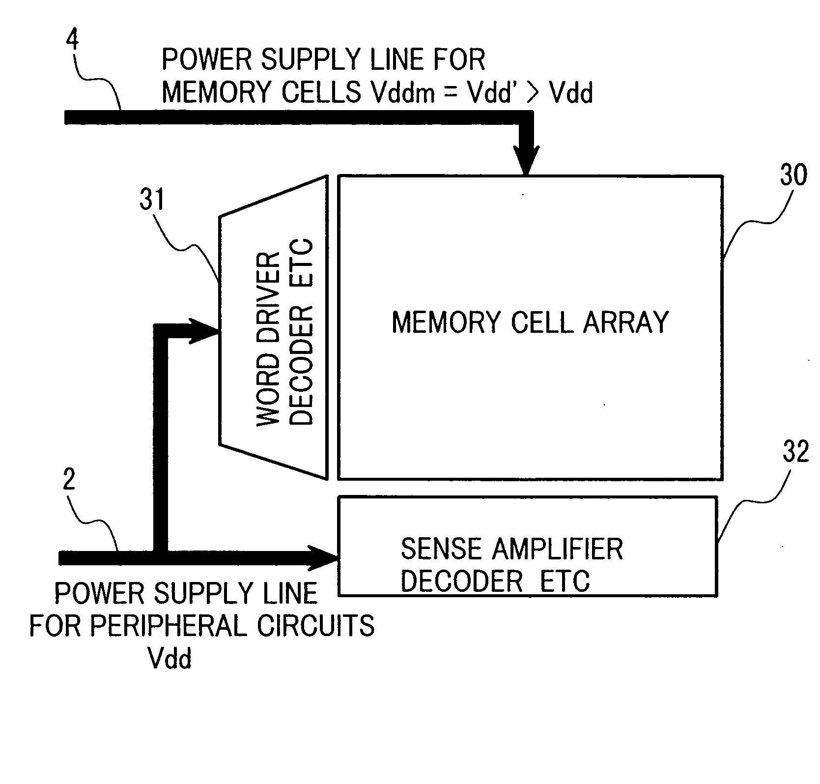
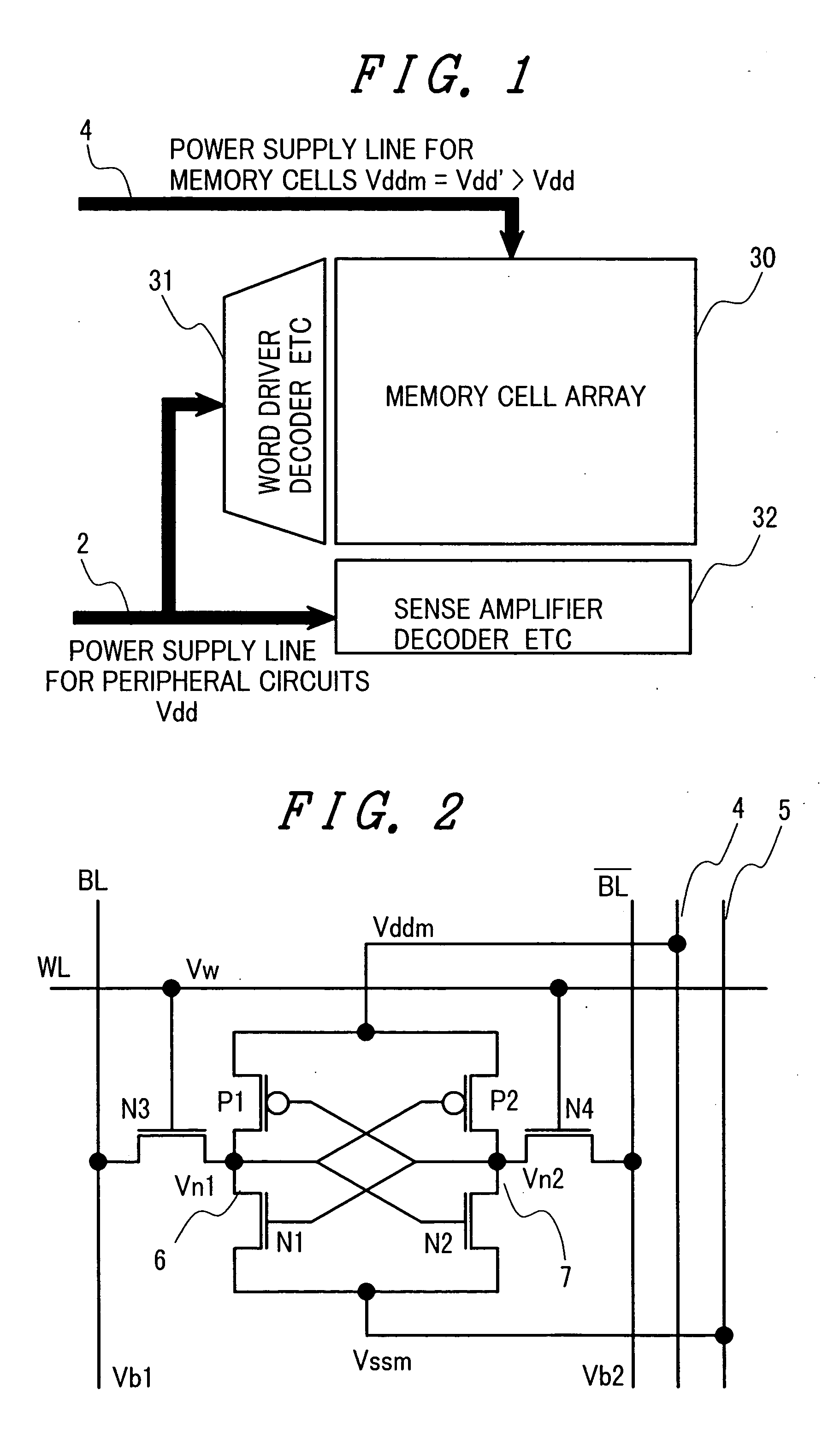
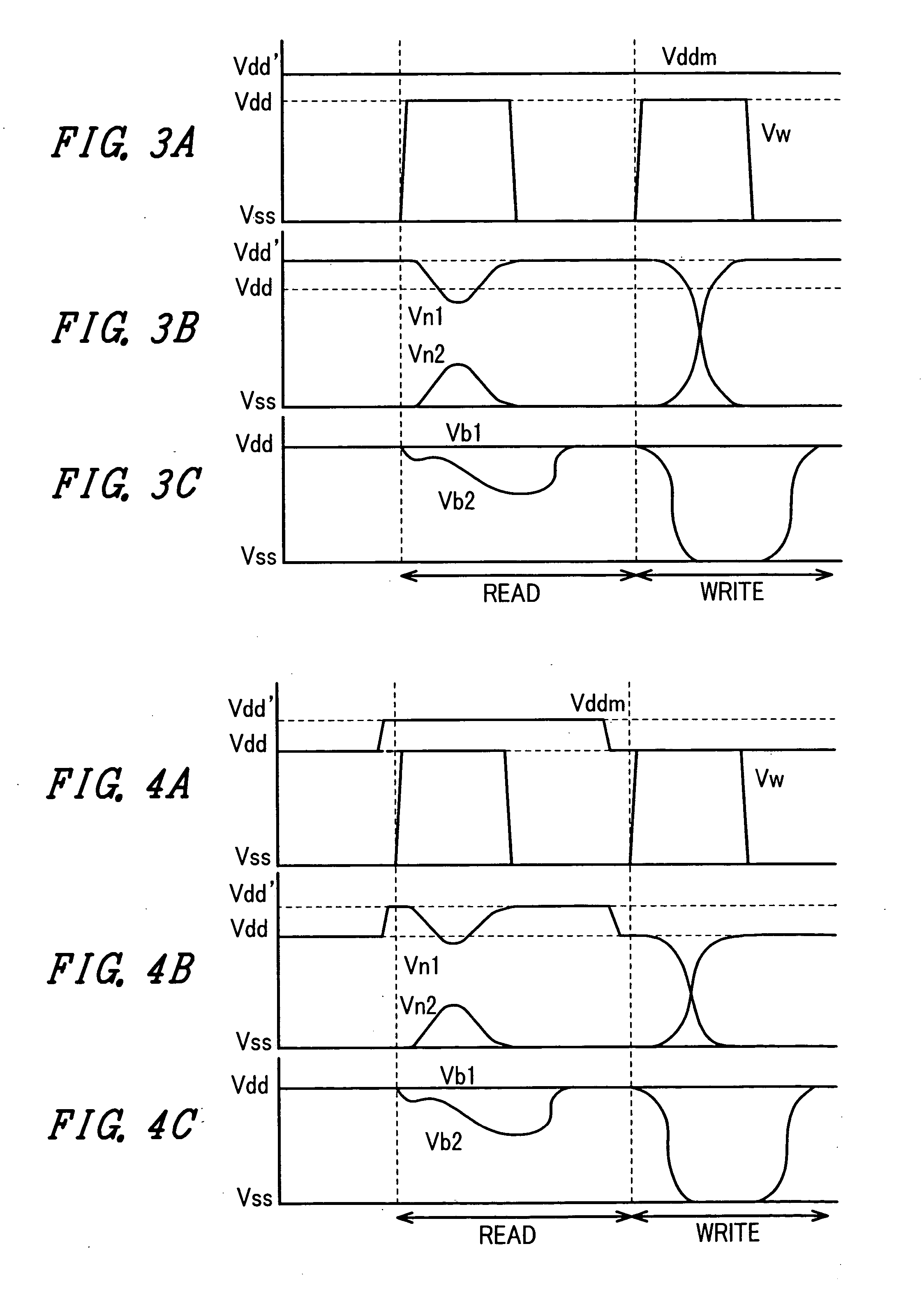
[0053]FIG. 1 is a block diagram showing a memory cell array 30 constituting a SRAM memory in accordance with the present invention, a peripheral circuit 31 of the memory including a word driver, a decoder, and the like, a peripheral circuit 32 of the memory including a sense amplifier, a decoder, and the like, and the relationship between respective voltages Vdd and Vddm of power supply lines 2 and 4 to be supplied to the memory cell array 30 and the peripheral circuits 31 and 32. A voltage Vdd′ higher than the voltage Vdd of the power supply line 2 for the peripheral circuits 31 and 32 other than the memory cell array is applied to the power supply line 4 for the memory cell array 30. Incidentally, the same ground voltage Vss is applied to the source line of memory cell driver MOS transistors in the memory cell array 30, and the ground lines for other peripheral circuits, which are not shown.

[0054] The configuration of the memory cell of the SRAM memory in thi...

embodiment 2

[0069] (Embodiment 2)

[0070]FIG. 5 shows another embodiment of the power supply configuration for the memory cell array constituting the SRAM memory in accordance with the present invention, and the peripheral circuits of the memory including a sense amplifier, a decoder, and the like. This configuration is different from the configuration of FIG. 1 described above in that the same voltage Vdd as that of the power supply line 2 for the peripheral circuits is applied as the voltage Vddm of the power supply line 4 for the memory array, and in that a voltage lower than a ground voltage Vss of a ground line 2s for the peripheral circuits other than the memory cell array is applied as a source line voltage Vssm of a memory cell driver MOS source line 5.

[0071] By keeping the source line voltage Vssm of the memory cell driver MOS transistors lower than the word line voltage Vw and the bit line voltages Vb1 and Vb2, the gate-source voltage of the driver MOS transistors N1 and N2 of the SRAM...

embodiment 3

[0072] (Embodiment 3)

[0073]FIG. 7 shows a still other embodiment of the power supply configuration for the memory cell array constituting the SRAM memory in accordance with the present invention, and the peripheral circuits of the memory including a sense amplifier, a decoder, and the like. This configuration is similar to the configuration of FIG. 5, but different therefrom in that the voltage Vdd′ higher than the power supply voltage Vdd for the circuits other than the memory cell array is coupled to the memory cell array 30 as the power supply voltage Vddm for the memory array.

[0074] Also with such a configuration, by keeping the memory array power supply voltage Vddm higher than the word line voltage Vw and the bit line voltages Vb1 and Vb2, and keeping the source line voltage Vssm of the memory cell driver MOS transistors lower than the word line voltage Vw and the bit line voltages Vb1 and Vb2, the gate-source voltage of the driver MOS transistors N1 and N2 of the SRAM cell b...


PUM


Abstract

A memory using an SRAM memory cell intended for low-voltage operation is designed to decrease the threshold value of MOS transistors constituting the memory cell without substantial decrease in the static noise margin, which is the operational margin of the memory cell. To this end, a voltage Vdd′ higher than a power supply voltage Vdd of a power supply line for peripheral circuits is supplied from a power supply line for memory cells as a power supply voltage for memory cells. Since the conductance of driver MOS transistors is increased, the threshold voltage of the MOS transistors within the memory cells can be reduced without reducing the static noise margin. Further the ratio of width between the driver MOS transistor and a transfer MOS transistor can be set to 1, thereby allowing a reduction in the memory cell area.

Description

BACKGROUND OF THE INVENTION [0001] 1. Field of the Invention [0002] The present invention relates to a semiconductor memory device. More particularly, it relates to a semiconductor memory device preferable for a SRAM (Static Random Access Memory) which has secured the operational margin during write operation, and operates at a low voltage and a low electric power. [0003] 2. Description of the Related Art [0004] In recent years, there has been an increasingly growing trend towards portable devices, which increases a demand for lower power consumption of a large-scale semiconductor integrated circuit (LSI). Therefore, a technology of an LSI operating at a voltage of not more than 1 V becomes necessary. In the future, presumably, there will be growing demands for a further decrease in supply voltage from that of an LSI operating at a supply voltage of about 0.9 V, so that an LSI operating even at a supply voltage of about 0.5 V will be demanded. [0005] For operating the LSI at a low v...

Claims


Application Information

Patent Timeline
Patent Type & Authority Applications(United States)
IPC IPC(8): G11C11/41G11C11/413G11C11/412G11C11/417H01L21/8244H01L27/10H01L27/11
CPCG11C11/412Y10S257/903G11C11/417
Inventor YAMAOKA, MASANAOOSADA, KENICHIISHIBASHI, KOICHIRO
Owner RENESAS ELECTRONICS CORP
Why Eureka
Try Eureka