Semiconductor memory device

a semiconductor and memory device technology, applied in the direction of redundant data error correction, fault response, instruments, etc., can solve the problems of increasing the delay of voltage signal transmission on such on-chip lead wires, requiring a longer read cycle time, and increasing the “wire delay”

Inactive Publication Date: 2005-02-03
KK TOSHIBA
View PDF6 Cites 48 Cited by
  • Summary
  • Abstract
  • Description
  • Claims
  • Application Information

AI Technical Summary

Benefits of technology

[0025] a control circuit used for timing control of data read of the memory cell array, for outputting at least

Problems solved by technology

Increasing the integration density of memory cell array by miniaturizing the cell size of NAND-EEPROM chips while lengthening data select lines for common connection of the control gates of memory cells, the data select lines (gate wiring leads) increase in electrical resistance, resulting in an increase in delay of voltage signal transmission on such on-chip lead wires-namely, “wire delay”-becomes greater.
Unfortunately, this serves as a bar for acceleration of read/write operations.
Unfortunately with prior art read methods for merely reading the cell units 49a to 49c together at a time, the actual read time is limited to the read time range T2 of NAND cell unit 49c. Thus a longer read cycle time is required.
Having stated abov

Method used


Image

  • Semiconductor memory device
  • Semiconductor memory device
  • Semiconductor memory device

Examples


embodiment 1

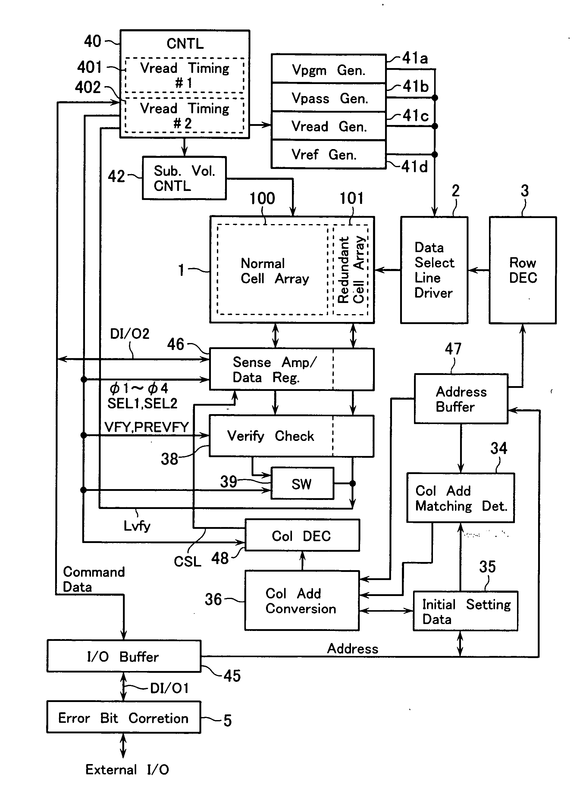
[0071]FIG. 1 illustrates, in functional block form, an internal configuration of an electrically erasable programmable read-only memory (EEPROM) chip in accordance with an embodiment of the invention.

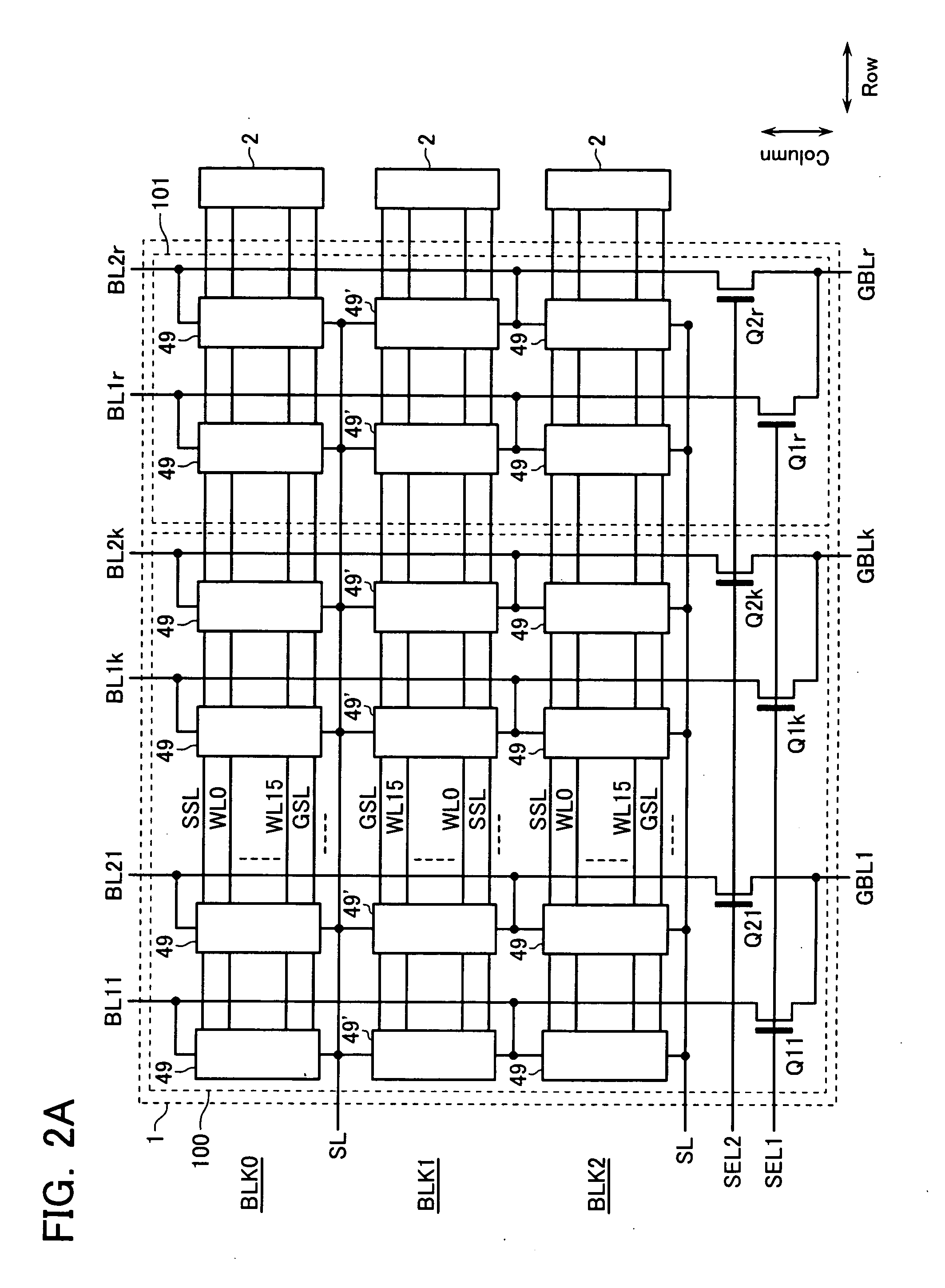
[0072] The illustrative EEPROM includes a memory cell array 1. The memory cell array 1 has a main cell array 100 which is referred to as a “normal data area” (first area) for storing therein the data as given from external input terminals I / O. The memory cell array 1 also has a redundant cell array 101 which is used as a “redundant area” (second area). The redundant cell array 101 is laid out on one end side of the normal cell array 100 along the row direction—that is, at a specific location in close proximity to a data select line driver 2 which drives data select lines of the memory cell array 1.

[0073] In the case of this embodiment, the redundant cell array 101 is a “redundant area” for use as a spare column cell area used for replacement of a column of the normal cell array 100 wh...

embodiment 2

[0174] Turning to FIG. 13, an EEPROM chip in accordance with an embodiment 2 of the invention is shown in a functional block form. The same parts or components and the same voltages to those of the embodiment 1 stated supra are denoted by the same reference characters, with detailed explanations thereof eliminated herein. In this embodiment, the column address conversion circuit 36 for performing defective column replacement additionally has therein specific logical / physical column address functionality, which exchanges or “interchanges” the order of sequence of at least part of physical column addresses to be sequentially selected by logical column addresses. With this built-in functionality of the column address converter circuit 36, it becomes possible to finally output the data of a specified storage area which is in the middle of a series of columns, when consecutively outputting data bits of multiple columns within the memory cell array 1. These functions will be explained in ...

embodiment 3

[0220]FIG. 22 shows a functional block configuration of an EEPROM in accordance with an embodiment 3 of the invention. FIG. 23A shows a configuration of a memory cell array 1, while FIG. 23B shows internal configurations of a sense amplifier circuit 46 and verify check circuit 38. Parts or components corresponding to those of the embodiments 1-2 stated supra are designated by the same reference characters with detailed explanations thereof eliminated herein. In this embodiment a column decoder circuit 48 is arranged to include therein a logical / physical column address conversion circuit added thereto. The logical / physical column address conversion function as used herein is for causing a certain redundancy cell array adjacent to data select line driver 2a, 2b to be last selected under a condition determined by the relationship in layout between a memory cell array 1 and data select line driver 2a, 2b. In brief, the logical / physical column address conversion function added to column ...


PUM


Abstract

A semiconductor memory device includes: a memory cell array having a plurality of data select lines disposed in parallel with each other, a plurality of data transfer line disposed in parallel with each other to intersect the data select lines, and electrically rewritable memory cells laid out at cross portions between the data select lines and data transfer lines; a data select line driver for driving the data select lines of the memory cell array; a sense amplifier circuit connected to the data transfer lines of the memory cell array, for performing data read of memory cells selected by one of the data select lines; and a control circuit used for timing control of data read of the memory cell array, for outputting at least two types of timing signals as being different in accordance with a selected data area of the memory cell array.

Description

CROSS-REFERENCE TO RELATED APPLICATIONS [0001] This application is based on and claims the benefit of prior Japanese Patent Application No. 2003-204508, filed on Jul. 31, 2003 and prior Japanese Patent Application No. 2003-328742, filed on Sep. 19, 2003, the entire contents of which are incorporated herein by reference. BACKGROUND OF THE INVENTION [0002] 1. Field of the Invention [0003] This invention relates to an electrically rewritable semiconductor memory device. [0004] 2. Description of the Related Art [0005] Various types of electrically rewritable non-volatile semiconductor memory devices including electrically erasable programmable read-only memory (EEPROM) chips have been developed. Memory cells of the type having metal oxide semiconductor field effect transistor (MOSFET) structures are such that each cell stores as digital bit information electrical charge which was injected from a channel into a charge accumulation or storage layer through an insulative film by the flow o...

Claims


Application Information

Patent Timeline
IPC IPC(8): G06F11/10G11C16/02G11C8/00G11C11/34G11C16/00G11C16/04G11C16/06G11C16/10G11C16/26G11C16/32G11C16/34G11C29/00G11C29/04G11C29/42G11C29/52H01L21/8247H01L27/00H01L27/115H01L29/788H01L29/792
CPCG06F11/1008G06F11/108G11C16/04G11C16/0483G11C16/26G11C16/32G11C16/3454G11C29/50004G11C29/52G11C29/76G11C29/82G11C29/84G11C2029/0409H01L27/115H01L27/11521H01L27/11524G11C7/22H10B69/00H10B41/30H10B41/35G11C16/00H01L27/00G11C16/10
Inventor NOGUCHI, MITSUHIROGODA, AKIRANITTA, HIROYUKI
Owner KK TOSHIBA
Why Eureka
Try Eureka