Manufacturing method of semiconductor device
- Summary
- Abstract
- Description
- Claims
- Application Information
AI Technical Summary
Benefits of technology
Problems solved by technology
Method used
Image

Examples
Embodiment Construction
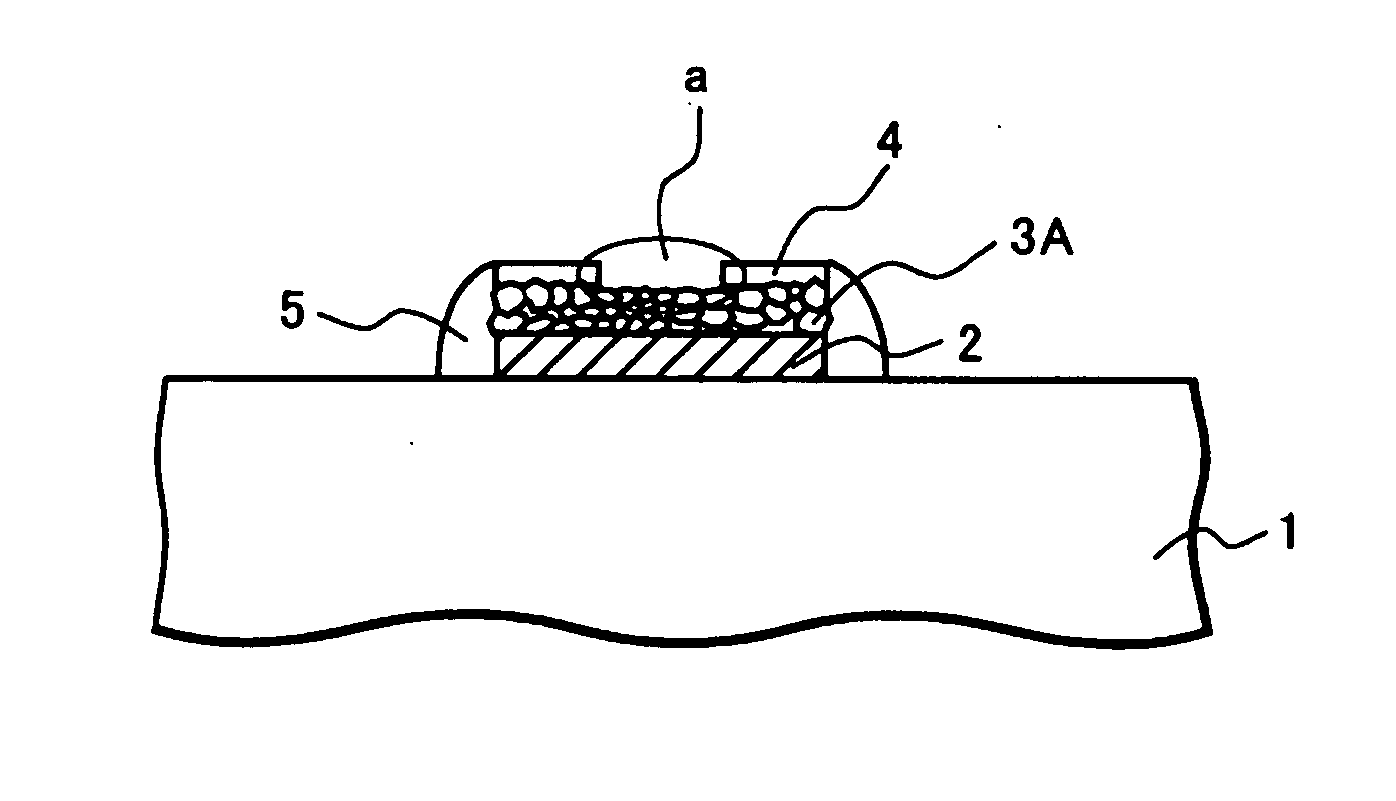
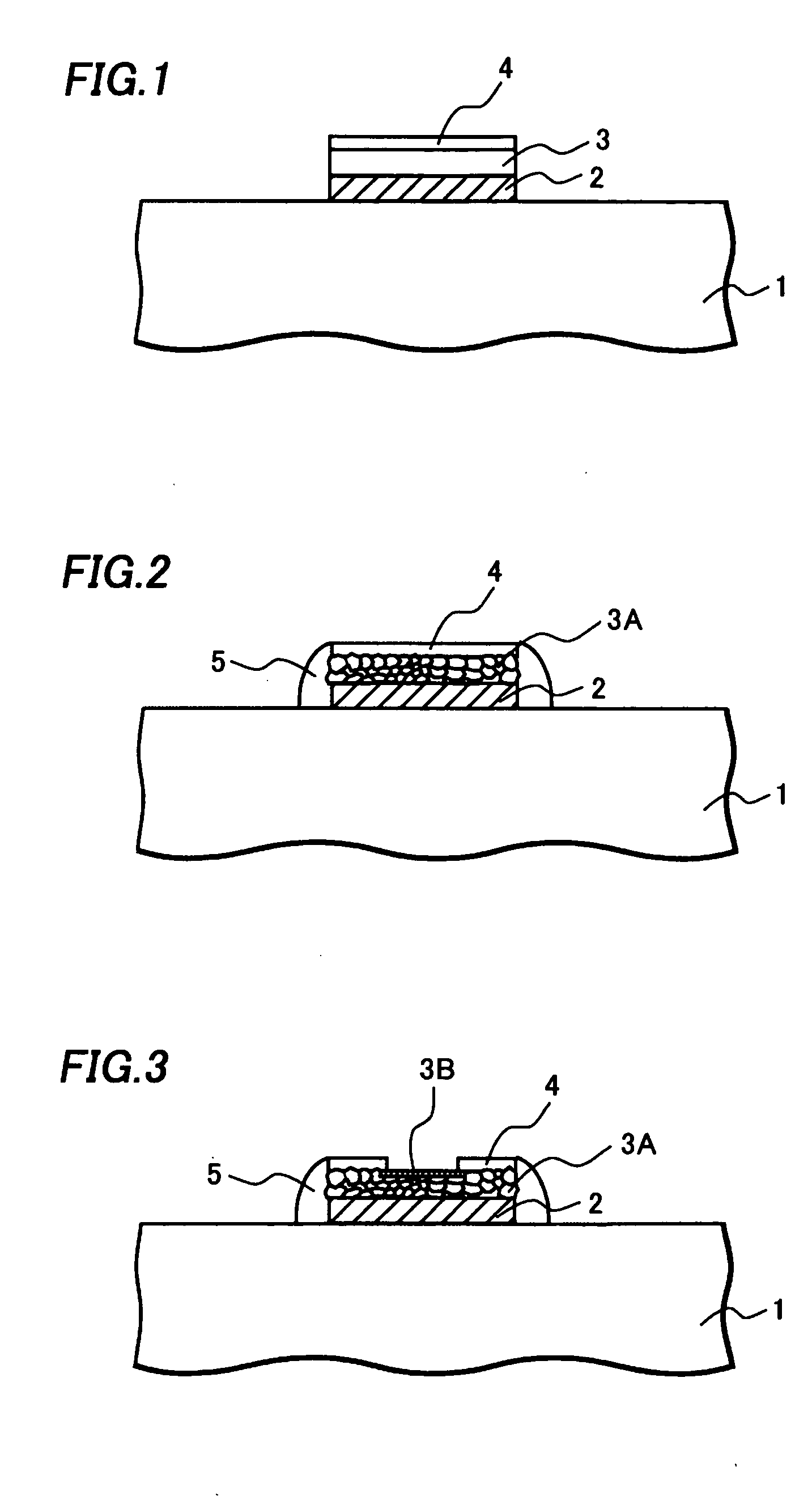
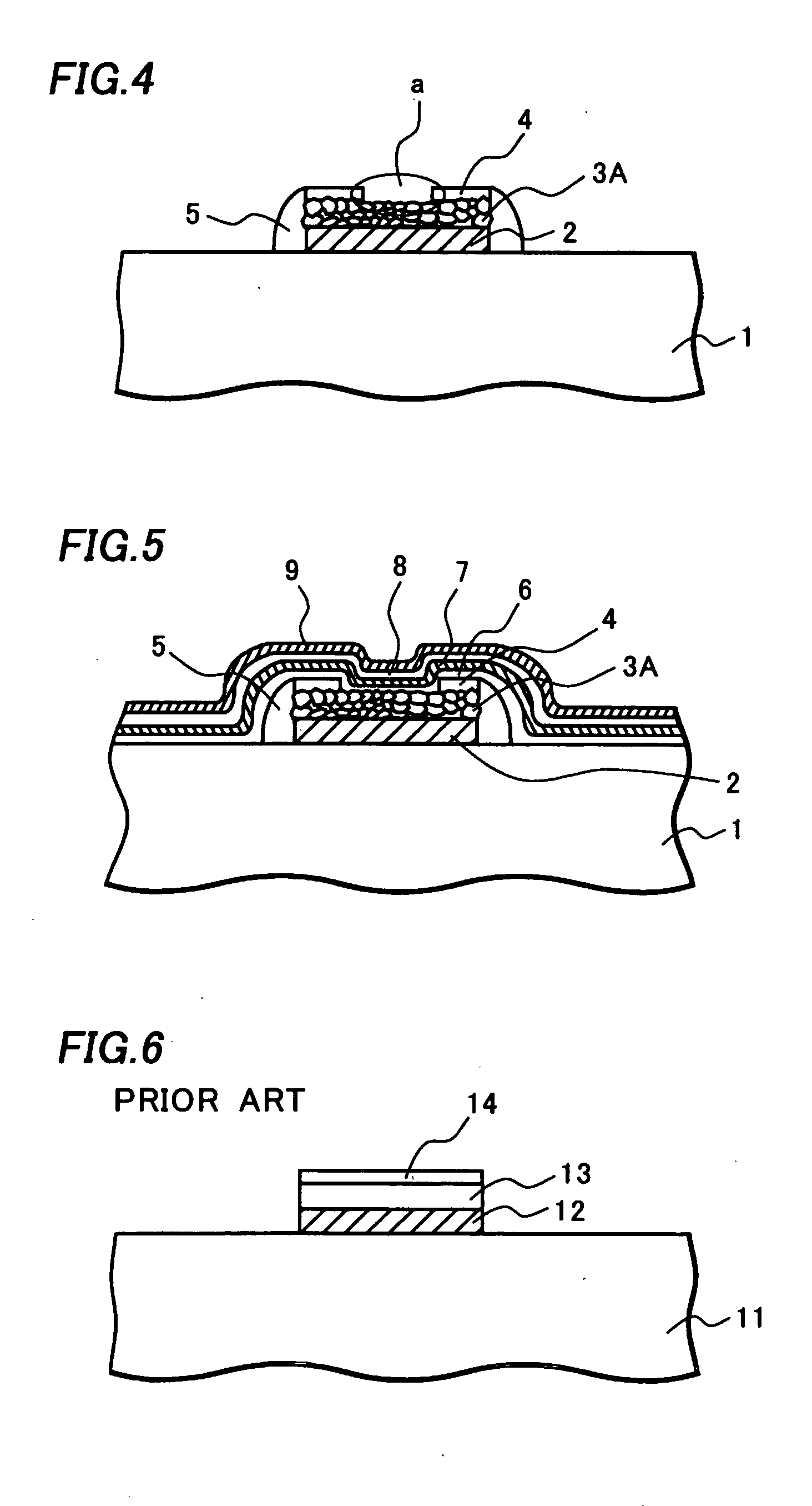
[0021] The quantity of electric charge stored in the capacitive element is represented by a product of capacitance of the capacitive element and a voltage applied to the capacitive element. The capacitance is represented by a dielectric constant of the dielectric film multiplied by an area of the electrode of the capacitive element divided by a distance between the electrodes.
[0022] In order to increase the quantity of stored electric charge while keeping small dimensions, it is conceivable that a material having a higher dielectric constant is chosen and used as the dielectric film. However, changing the dielectric film material is not regarded as the best solution when the cost of alternative materials and the equipment suitable for those materials are taken into consideration.
[0023] With this being the situation, the inventor has tried to work out a method to improve the breakdown voltage of the dielectric film. If the breakdown voltage of the dielectric film is successfully in...
PUM
 Abstract
Description
Claims
Application Information
 - Generate Ideas
- Intellectual Property
- Life Sciences
- Materials
- Tech Scout
- Unparalleled Data Quality
- Higher Quality Content
- 60% Fewer Hallucinations
Browse by: Latest US Patents, China's latest patents, Technical Efficacy Thesaurus, Application Domain, Technology Topic, Popular Technical Reports.
© 2025 PatSnap. All rights reserved.Legal|Privacy policy|Modern Slavery Act Transparency Statement|Sitemap|About US| Contact US: help@patsnap.com