

Semiconductor device and method of manufacturing semiconductor device
a semiconductor and semiconductor technology, applied in semiconductor lasers, instruments, optical elements, etc., can solve the problem that crystals cannot be pumped by current injection
- Summary
- Abstract
- Description
- Claims
- Application Information
AI Technical Summary
Benefits of technology
Problems solved by technology
Method used
Image

Examples
first embodiment
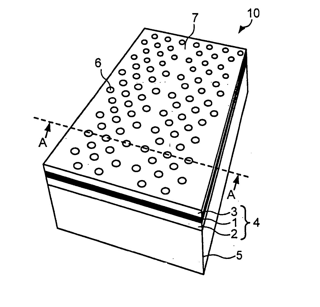
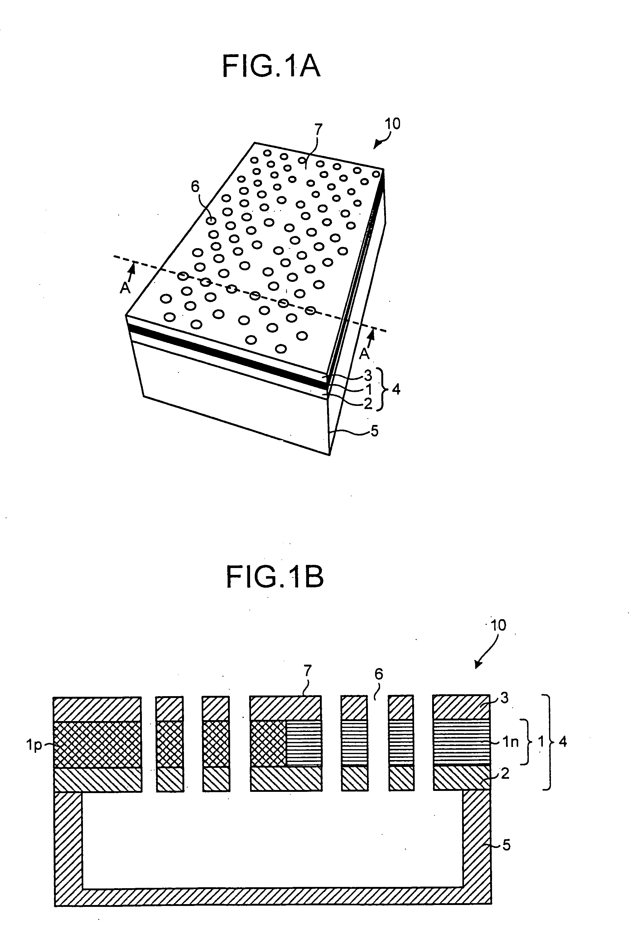
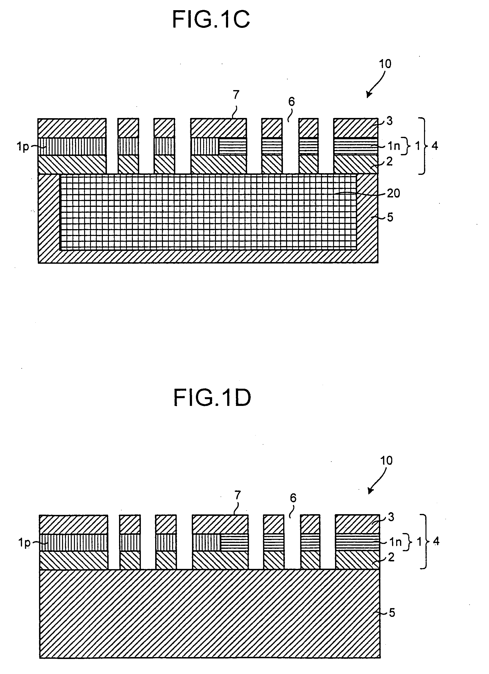
[0025]FIG. 1A and FIG. 1B typically illustrate a semiconductor device 10 according to the present invention. FIG. 1A is a perspective view, and FIG. 1B is a cross-sectional view, taken along a line A-A shown in FIG. 1A, of the semiconductor device 10.
[0026] The semiconductor device 10 is constituted based on a two-dimensional slab photonic crystal structure. In the semiconductor device 10, a slab layer 4 is formed by sequentially stacking a lower cladding layer 2, an active layer 1, and an upper cladding layer 3 on a substrate 5, an interior of which is hollow, and a periodic refractive index profile structure is formed in a two-dimensional plane of the slab layer 4. In the example of FIG. 1A and FIG. 1B, a triangular lattice-like air hole structure 6 is formed, as the periodic refractive index profile structure formed on the slab layer 4, to penetrate the slab layer 4 in a stack direction. A linear defect (waveguide 7) for the periodic air hole structure 6 in the two-dimensional pl...
second embodiment
[0045] Furthermore, as shown in FIG. 5B, if the upper cladding layer 3 is a cladding layer doped with the p-type dopant and the lower cladding layer 2 is a cladding layer doped with the n-type dopant, the current can be efficiently carried to the pn junction section in the active layer 1. If so, by using at least one of boundaries between the active layer 1 and the upper cladding layer 3 and between the active layer 1 and the lower cladding layer 2 as a waveguide part, it is possible to easily concentrate the current on the waveguide part of active layer 1 and to realize efficient lasing. By using both of the boundaries between the active layer 1 and the upper cladding layer 3 and between the active layer 1 and the lower cladding layers 2 as the waveguide part and arranging the upper and lower cladding layers 2 and 3 so that cross sections thereof are diagonal to each other as shown in the cross section of FIG. 2B and FIG. 2C, it is possible to more easily concentrate the injection ...
third embodiment
[0047]FIG. 6A to FIG. 6C are cross-sectional views of a semiconductor device 60 according to the present invention. The semiconductor device 60 is characterized in that the ohmic contact layer 9 made of InGaAs or the like is formed, as an uppermost layer, between the two-dimensional slab photonic crystal (upper cladding layer 3) and electrodes 8 so as to have ohmic contact between the electrodes 8 and the slab layer 4. However, if the ohmic contact layer 9 is left on an upper portion of a laser light emission section, the ohmic contact layer 9 functions as an optical absorption layer. Therefore, it is necessary to remove the ohmic contact layer 9 from the periodic two-dimensional refractive index profile structure. As shown in FIGS. 6B and 6C, another ohmic contact layer 9b may be formed under the lower cladding layer 2. As shown in FIG. 6B, a cross section of the n-type electrode 8n-side semiconductor device 60 ranging from the substrate 5 to the upper cladding layer 3 may be expos...
PUM
 Abstract
Description
Claims
Application Information