Magnetic memory apparatus and method of manufacturing magnetic memory apparatus

a magnetic memory and memory device technology, applied in the direction of solid-state devices, basic electric elements, instruments, etc., can solve the problems of inability to apply to a finer wiring, inability to achieve a higher integration, drawbacks, etc., to achieve the effect of reducing current value, reducing wiring area, and improving the use efficiency of the magnetic field generated by the second wiring

Inactive Publication Date: 2005-02-10
SONY CORP
View PDF3 Cites 11 Cited by
  • Summary
  • Abstract
  • Description
  • Claims
  • Application Information

AI Technical Summary

Benefits of technology

[0023] According to the aforementioned second method of manufacturing the magnetic memory apparatus, the step of forming the second wiring includes the step of forming the second wiring in the memory cell region and the step of forming the second wiring in the peripheral circuitry region. In the step of forming the second wiring in the memory cell region, because that the second wiring is formed to have the magnetic material layer including the high magnetic permeability layer on both side surfaces and on the top surface opposite to its surface of the second wiring on the side facing the memory device, utilization efficiency of the magnetic field generated by the second wiring is improved by means of the magnetic material layer, thereby providing a structure capable of reducing a value of current for writing to the memory device. Moreover, because that the step of forming the second wiring in the memory cell region and the step of forming the second wiring in the peripheral circuitry region are performed by different steps, the magnetic material layer for cladding the wiring can be formed only in the memory cell region, avoiding forming thereof in the peripheral circuitry region. Therefore, the second wiring in the peripheral circuitry region can be integrated more densely that much corresponding to the elimination of the magnetic material layer cladding the wiring therein. In other words, according to elimination of a reduced wiring area due to the formation of the magnetic material layer, a wiring resistance can be reduced that much corresponding to a thus increased wiring area. Thereby, a wiring structure capable of reducing power consumption and a quantity of heat generation is fabricated.
[0024] As described heretofore, according to a magnetic memory apparatus in accordance with an embodiment of the present invention, because that the magnetic material layer including the high magnetic permeability layer is formed on the both side walls of the first wiring and on the rear surface opposite to the surface thereof facing the memory device only in the memory cell region, the efficiency of uti...

Problems solved by technology

However, while it is possible to improve a magnetic field efficiency and lower a value of current for writing to the device by use of the clad structure, on the other hand, if this process of cladding the circumferences of wiring with the magnetic material layer is applied to a peripheral circuitry region other than the memory cell, because of an ...

Method used


Image

  • Magnetic memory apparatus and method of manufacturing magnetic memory apparatus
  • Magnetic memory apparatus and method of manufacturing magnetic memory apparatus
  • Magnetic memory apparatus and method of manufacturing magnetic memory apparatus

Examples


second embodiment

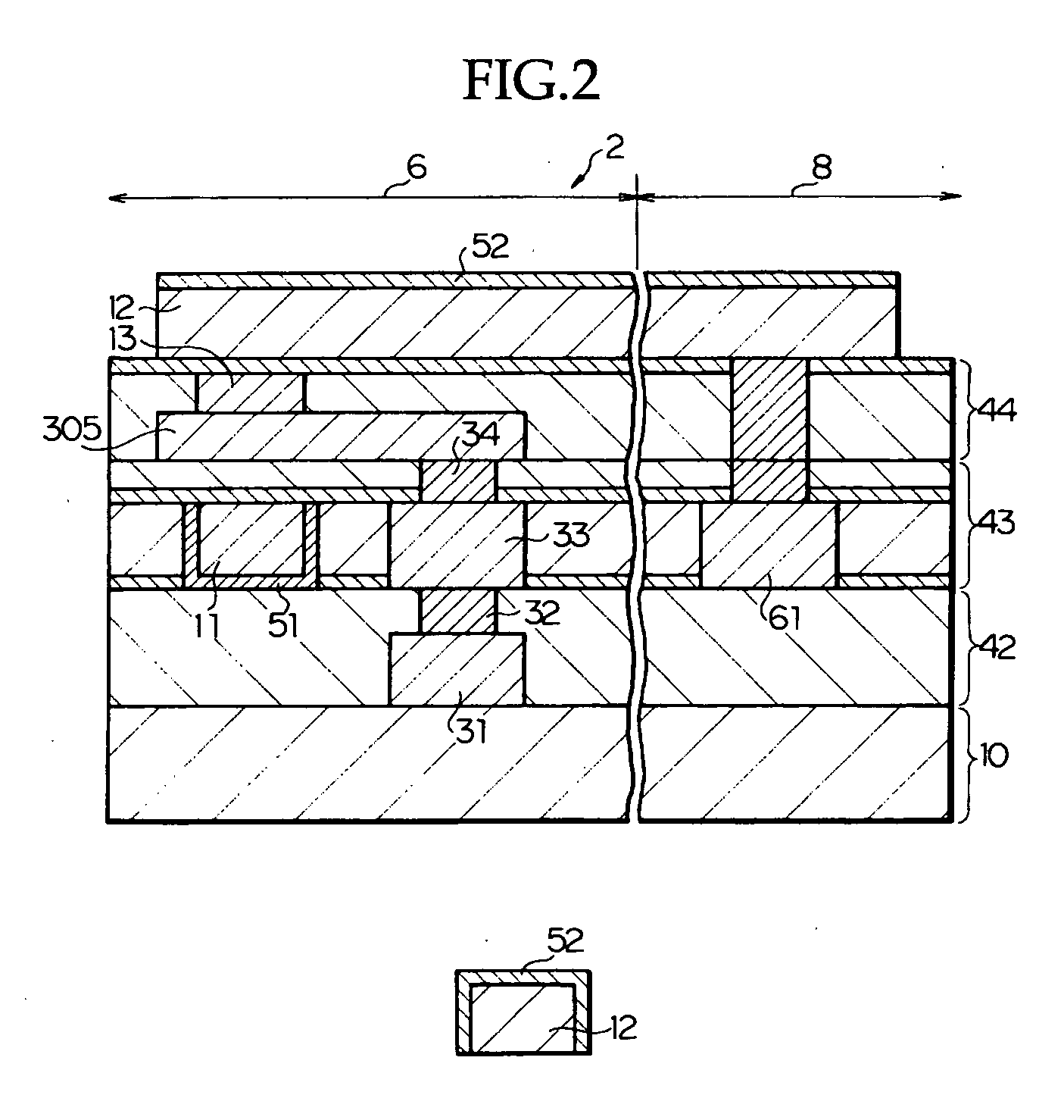
[0052] By referring to FIG. 2, which illustrates a schematic structural cross-section, a magnetic memory apparatus according to the present invention will be described. FIG. 2(2) illustrates a cross-section of a bit line in a width direction, which is to be formed in a memory cell region 6 in FIG. 2(1).

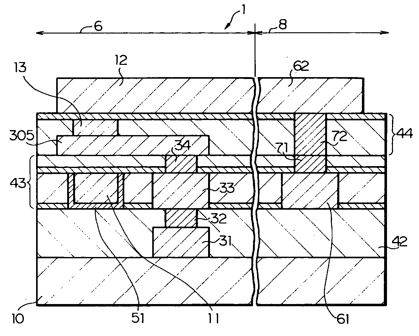
[0053] According to the second embodiment of the present invention, in order that a current magnetic field generated by a bit line (second wiring) in a memory cell region 6 is efficiently concentrated into a memory layer, a magnetic material layer is formed, and then in a peripheral circuitry region 8, second wiring without forming the magnetic material layer is disposed.

[0054] As shown in FIG. 2, there is provided a semiconductor device substrate 10 formed with devices, wiring, insulation films and the like. On this semiconductor device substrate 10, for example, a p-type well region is formed on the surface side of the semiconductor substrate (e.g. p-type semiconductor substrate), ...

first embodiment

[0056] On the aforementioned first insulation film there is formed a second insulation film 42. The second insulation film 42 in the memory cell region 6 covers the aforementioned sense line, connection electrode 31 and the like. Further, in the second insulation film 42 there is formed a contact (for example, a tungsten plug) 32 connected with the aforementioned connection electrode 31. Furthermore, on the second insulation film 42 there are formed a connection electrode 33 connected with the contact 32, a write word line 11 as the first wiring and the like. It is more preferable to provide a magnetic material layer 51 made from a high magnetic permeability layer so as to surround both side walls of the writing word line 11 and the bottom surface opposite to the upper surface thereof opposing a tunnel magnetoresistance device (hereinafter referred to as TMR) as described in the first embodiment, nevertheless it is still possible to write information to memory device 13 by the write...

third embodiment

[0120] According to the method of manufacturing the magnetic memory apparatus at the time of forming the wiring trench 453 for forming the second wiring (bit line) 12 in the fifth insulation film 45, etching is stopped by the stopper insulation film 451 which covers the cap layer 133. Then, after sequentially forming the first barrier metal layer 55 and the magnetic material layer 521 on the internal wall of the wiring trench 453 and on the surface of the fifth insulation film 45, the magnetic material layer 521, the first barrier metal layer 55 and the stopper insulation film 451 in the bottom of the wiring trench 453 are removed to expose the upper surface of the cap layer 133, and also the magnetic material layer 521 and the first barrier metal layer 55 on the fifth insulation film 45 are removed, so that the side wall of the magnetic material layer 521 is formed along the side wall of the wiring trench 453 via the first barrier metal layer 55. At this time, the upper surface of...


PUM


Abstract

A magnetic memory apparatus including a memory cell region and a peripheral circuitry region mounted on a substrate is provided. The memory cell region includes first wiring, second wiring that three-dimensionally intersects with the first wiring, and a magnetoresistance effect type memory device disposed in an intersecting region of the first and the second wiring for storing and reproducing information of a magnetic spin. The peripheral circuitry region includes first wiring that is in the same wiring layer as that of the first wiring in the memory cell region, and second wiring that is in the same wiring layer as the second wiring in the memory cell, and a magnetic material layer including a high magnetic permeability layer is formed on both side surfaces of the first wiring only within the memory cell region and on a surface opposite to a surface facing the memory device.

Description

CROSS REFERENCES TO RELATED APPLICATIONS [0001] The present invention claims priority to its priority document No. 2003-161451 filed in the Japanese Patent Office on Jun. 6, 2003, the entire contents of which being incorporated by reference herein. BACKGROUND OF THE INVENTION [0002] 1. Field of the Invention [0003] The present invention relates to a magnetic memory apparatus and a method of manufacturing a magnetic memory apparatus, and more particularly to a nonvolatile type magnetic memory apparatus and a method of manufacturing a magnetic memory apparatus which stores information by utilizing a change in a resistance value depending on spin orientation in a ferromagnetic material, which can be parallel or anti-parallel. [0004] 2. Description of Related Art [0005] With a rapid prevalence of information communication equipment, in particular, of personal compact equipment such as portable telephones, a still more improved performance such as a higher circuit integration, faster spe...

Claims


Application Information

Patent Timeline
IPC IPC(8): G11C11/00H01L21/3205G11C11/15G11C11/16H01L21/8246H01L23/52H01L27/10H01L27/105H01L43/08
CPCG11C11/16H01L43/12H01L43/08H10N50/10H10N50/01G11C11/15
Inventor TAI, KAORI
Owner SONY CORP
Why Eureka
Try Eureka