Method to pattern a substrate

a substrate and workpiece technology, applied in the field of workpiece patterning, can solve the problems of mask error enhancement factor, high price of manufacturing masks, and high cost of masks, and achieve the effect of precise critical dimension

Active Publication Date: 2005-02-10
MICRONIC LASER SYST AB
View PDF13 Cites 2 Cited by
  • Summary
  • Abstract
  • Description
  • Claims
  • Application Information

AI Technical Summary

Benefits of technology

[0011] Accordingly, it is an object of the present invention to provide a meth

Problems solved by technology

More recently, the need to manufacture integrated circuits by means other than using a conventional mask has developed for a number of reasons, for example the price of manufacturing mask(s) has increased due to its complexity to manufacture, small-scale development which needs very small series of integrated circuits, etc.
However, a difference in criticality is much less than mi

Method used


Image

  • Method to pattern a substrate
  • Method to pattern a substrate
  • Method to pattern a substrate

Examples


Embodiment Construction

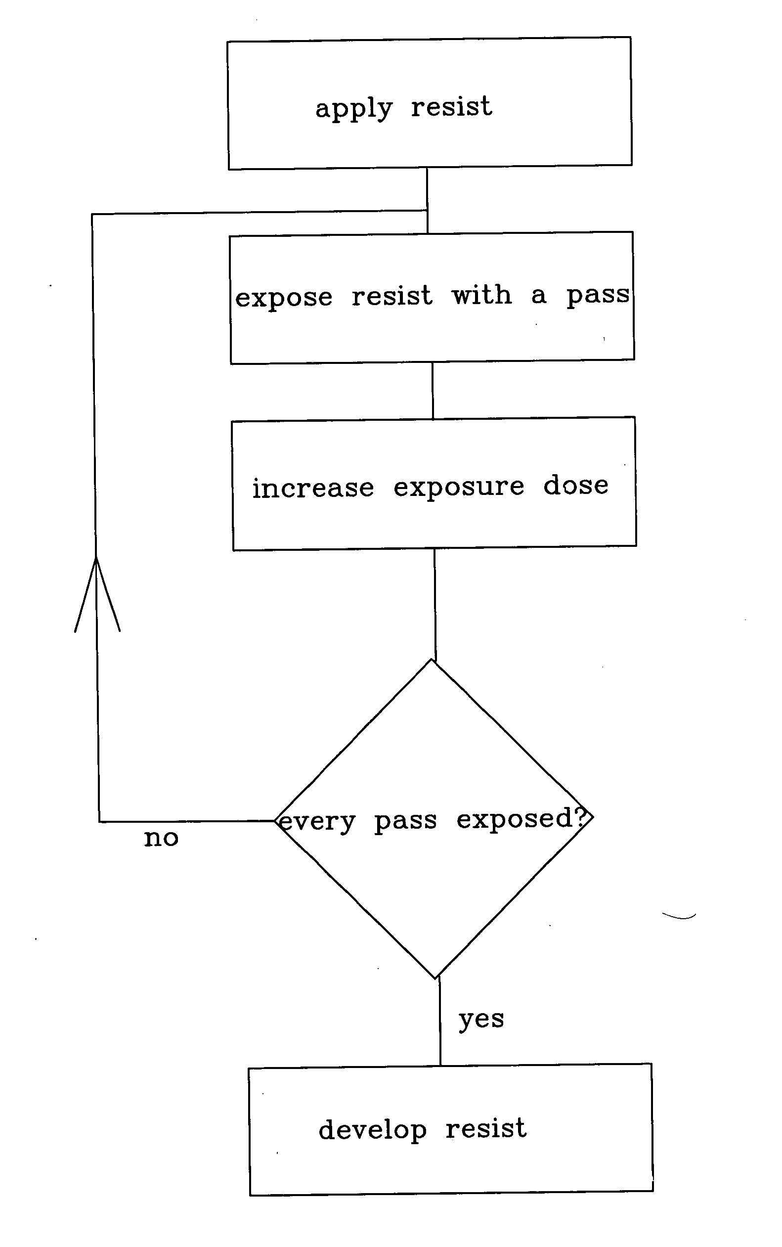
[0016] The following detailed description is made with reference to the figures. Preferred embodiments are described to illustrate the present invention, not to limit its scope, which is defined by the claims. Those of ordinary skill in the art will recognize a variety of equivalent variations on the description that follows.

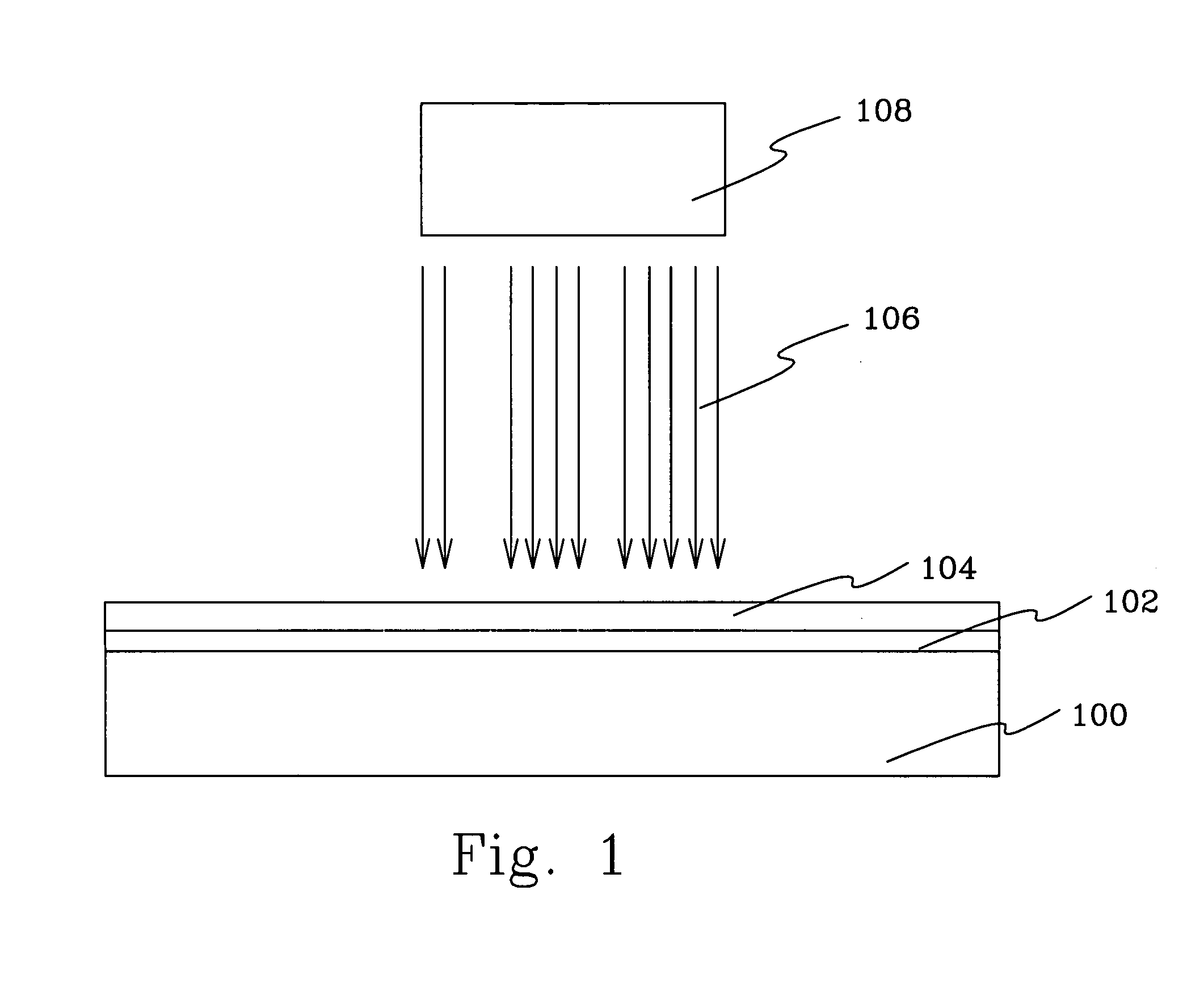
[0017]FIG. 1 depicts a coated substrate 100 comprising a masking or non-transmissive layer 102 and a resist layer 104. The substrate 100 may be a quarts substrate, an Erodent ceramic substrate or an ULE™ glass substrate when said substrate is to be a reticle or mask. However, when making integrated circuits by direct writing, said substrate may by any kind of semiconducting material. In such case the resist is applied directly onto said substrate.

[0018] The mask is formed over the transmissive substrate to block the passage of an energy beam in areas where resist on a wafer are intended not to be exposed. Unmasked portions of the substrate 100 allow an energy ...


PUM


Abstract

An aspect of the present invention includes a method of lithography to enhance uniformity of critical dimensions of features patterned onto a workpiece. Said workpiece is coated with a coating sensitive to electromagnetic radiation. An electromagnetic radiation source having an illumination intensity is provided. At least one object pixel of electromagnetic radiation is created. A predetermined pattern is exposed, by using said at least one object pixel, on at least a portion of said workpiece in a first exposure pass with a first dose to provide less than full exposure of said coating sensitive to electromagnetic radiation. Said exposing action is repeated at least until said portion of said coating sensitive to electromagnetic radiation is fully exposed, wherein said dose is increased for every following pass. Said fully exposed coating sensitive to electromagnetic radiation is developed.

Description

TECHNICAL FIELD [0001] The present invention relates to a method for patterning a workpiece in a lithographic process, in particular it relates to a method for improving the critical dimension uniformity. BACKGROUND OF THE INVENTION [0002] Semiconductor devices include multiple layers of structure. The structures are formed in numerous steps, including steps of applying resist, then exposing, developing and selectively removing the resist to from a pattern of exposed areas. The exposed areas may be etched to remove material or sputtered to add material. A critical part of forming the pattern in the resist is exposing it. Resist is exposed to an energy beam that changes its chemical properties. [0003] One way of exposing the resist is with a stepper. The stepper uses a reticle, which typically includes a carefully prepared, transmissive quartz substrate overlaid by a non-transmissive or masking layer that is patterned with areas to be exposed and areas to be left unexposed. Patternin...

Claims


Application Information

Patent Timeline
IPC IPC(8): G03C5/00G03F7/20
CPCG03F7/70558G03F7/70291G03C5/00G03F7/20
Inventor WALFORD, JONATHANASKEBJER, PEREKLUND, ROBERT
Owner MICRONIC LASER SYST AB
Why Eureka
Try Eureka