Reflective mask blank for EUV lithography

a lithography and reflective mask technology, applied in the field of euv lithography, can solve the problems of inability to use a refracting optical system, the conventional photolithography method is approaching its limit, and the miniaturization of semiconductor devices has been accelerated, so as to achieve excellent smoothness, improve the effect of edge roughness and free from deterioration of the pattern dimensional precision

Active Publication Date: 2011-10-04
ASAHI GLASS CO LTD
View PDF31 Cites 12 Cited by
  • Summary
  • Abstract
  • Description
  • Claims
  • Application Information

AI Technical Summary

Benefits of technology

[0041]The EUV mask blank of the present invention is characterized in that simply by adding inexpensive hydrogen gas (H2), it is possible to adjust the stress of the absorber layer, and the crystalline state of the absorber layer is amorphous, whereby the absorber layer surface is excellent in smoothness. As a result, a pattern to be formed on the absorber layer is free from an increase of edge roughness and free from deterioration of the dimensional precision of the pattern.
[0042]Further, at the time of producing the EUV mask blank, it is not necessary to use a complex mechanism such as a substrate-heating mechanism, a bias mechanism or an ion-assisting mechanism, whereby reduction of defects in the EUV mask blank to be produced, can be expected.

Problems solved by technology

However, the conventional photolithography method is approaching its limit, while miniaturization of semiconductor devices has been accelerated.
EUV light is likely to be readily absorbed by all materials, and the refractive indices of the materials at this wavelength are close to 1, whereby it is not possible to use a refracting optical system as used in a conventional photolithography employing visible light or ultraviolet light.

Method used


Image

  • Reflective mask blank for EUV lithography
  • Reflective mask blank for EUV lithography

Examples


example 1

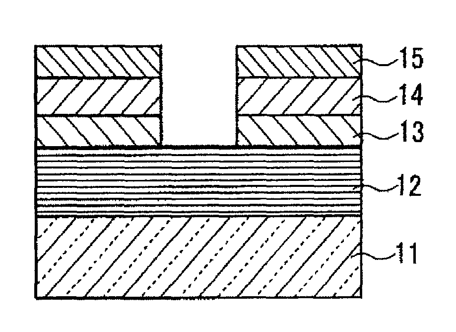
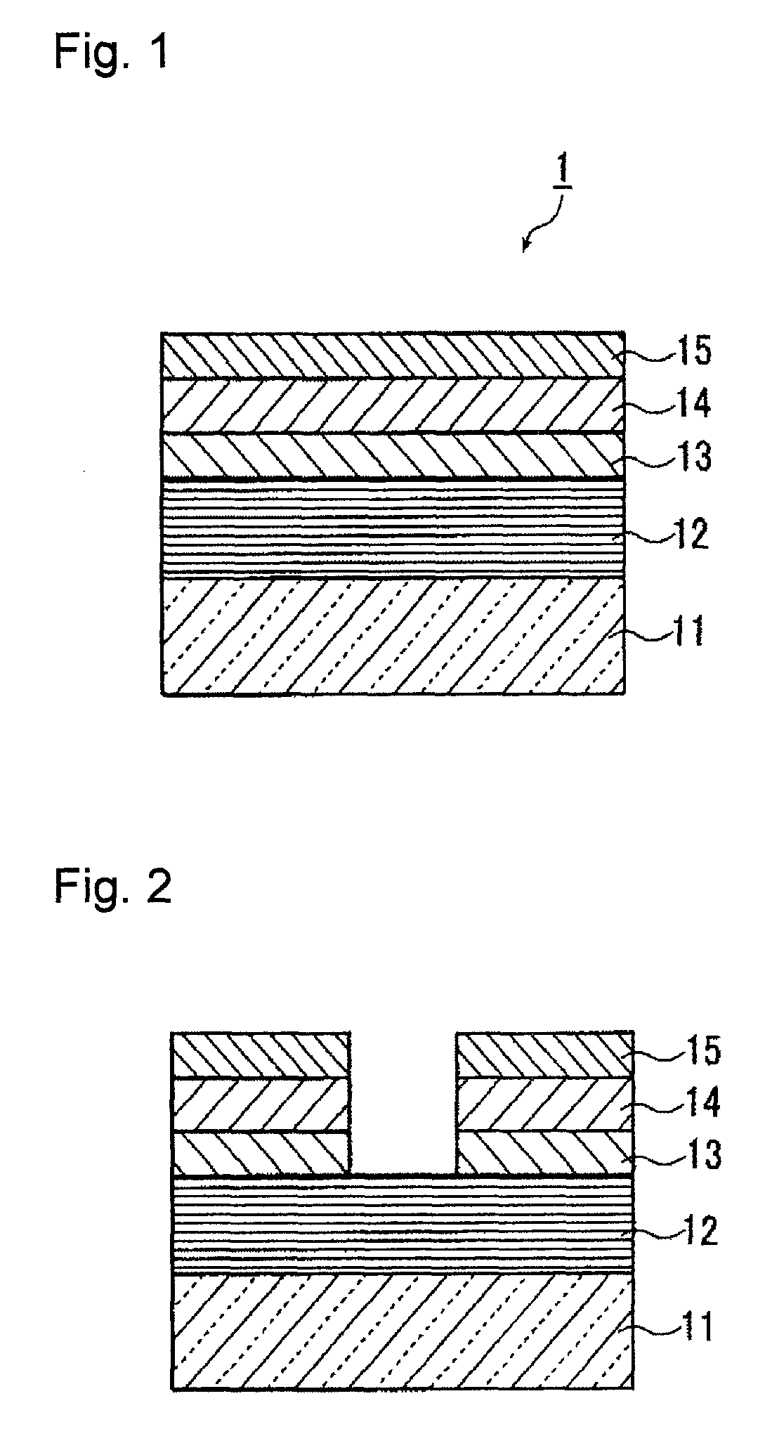
[0164]In this Example, an EUV mask blank as shown in FIG. 1 was prepared. However, in the EUV mask blank 1 in Example 1, no low reflection layer 15 was formed on an absorber layer 14. As a substrate 11 for film forming, a SiO2—TiO2 type glass substrate (shape: 6 inch (152 mm) square, thickness: 6.3 mm) was used. This glass substrate had a thermal expansion coefficient of 0.2×10⁻⁷ / ° C., a Young's modulus of 67 GPa, a Poisson's ratio of 0.17 and a specific rigidity of 3.07×10⁷ m2 / s2. This glass substrate was polished to form a smooth surface having a surface roughness (rms) of at most 0.15 nm with a flatness of at most 100 nm.

[0165]On the rear side of the substrate 11, a conductive film having a sheet resistance of 70Ω / □ was applied by forming a CrN film having a thickness of 100 nm by using a magnetron sputtering method.

[0166]On a flat-plate-form usual electrostatic chuck, a substrate 11 (shape: 6 inch (152 mm) square, thickness: 6.3 mm) was fixed via the formed CrN film, and on the ...

example 2

[0222]In this Example, an EUV mask blank 1 having a low reflection layer 15 (TaON film) containing Ta, N and O formed on an absorber layer 14 (TaNH film) was prepared.

[0223]In this Example, the procedure up to forming an absorber layer 14 on the protective layer 13 was carried out in the same manner as in Example 1. On the absorber layer 14, a low reflection layer containing Ta, N and O was formed as a low reflection layer 15 to an inspection light with an wavelength of 257 nm, by using a magnetron sputtering method. The compositional ratio (at %) of the low reflection layer was Ta:N:O=22.1:4.4:73.5, as measured by the same method as in Example 1.

[0224]The film-forming conditions for the low reflection layer 15 (TaON film) were as follows.

Film-Forming Conditions for Low Reflection Layer 15 (TaON Film)

[0225]Target: Ta target

[0226]Sputtering gas: Mixed gas of Ar, N2 and O2 (Ar: 36 vol %, N2: 14 vol %, O2: 50 vol %, gas pressure: 0.3 Pa)

[0227]Applied power: 450 W

[0228]Film-forming rate...

example 3

[0233]Example 3 was carried out in the same manner as in Example 1 except that the absorber layer 14 (TaNH) was formed under the following conditions.

[0234]The film-forming conditions for the absorber layer 14 were as follows.

Film-Forming Conditions for Absorber Layer 14 (TaNH Film)

[0235]Target: Ta target

[0236]Sputtering gas: Mixed gas of Ar, N2 and H2 (Ar: 78.0 vol %, N2: 11.1 vol %, 10.9 vol %, gas pressure: 0.36 Pa)

[0237]Applied power: 300 W

[0238]Film-forming rate: 1.3 nm / min

[0239]Film thickness: 60 nm

[0240]The composition of the absorber layer 14 (TaNH) was measured in the same manner as in Example 1, whereby the compositional ratio (at %) of the absorber layer 14 (TaNH) was found to be Ta:N:H=53.4:36.6:10.0 (Ta content: 53.4 at %, N content: 36.6 at %, H content: 10.0 at %). The crystalline state of the obtained absorber layer 14 is confirmed by using an X-ray diffraction apparatus, whereby no sharp peak is observed among the obtained diffraction peaks, and it is confirmed that...


PUM

PropertyMeasurementUnit
surface roughnessaaaaaaaaaa
thicknessaaaaaaaaaa
thicknessaaaaaaaaaa

Abstract

A reflective mask blank for EUV lithography is provided which has an absorber layer wherein stress and crystal structure can be easily controlled.A reflective mask blank for EUV lithography, which comprises a substrate, and at least a reflective layer for reflecting EUV light and an absorber layer for absorbing EUV light formed in this order on the substrate, wherein the absorber layer contains tantalum (Ta), nitrogen (N) and hydrogen (H); and in the absorber layer, the total content of Ta and N is from 50 to 99.9 at %, and the content of H is from 0.1 to 50 at %.

Description

TECHNICAL FIELD[0001]The present invention relates to a reflective mask blank for EUV (Extreme Ultraviolet) lithography (hereinafter referred to as “an EUV mask blank” in this specification) to be used for e.g. production of semiconductors.BACKGROUND ART[0002]Heretofore, in the semiconductor industry, a photolithography method employing visible light or ultraviolet light has been used as a technology to transfer a fine pattern required for forming an integrated circuit made of a fine pattern on e.g. a Si substrate. However, the conventional photolithography method is approaching its limit, while miniaturization of semiconductor devices has been accelerated. In the case of the photolithography method, the resolution limit of a pattern is at a level of ½ of the exposure wavelength, and even when a liquid immersion method is employed, it is said to be at a level of ¼ of the exposure wavelength. Accordingly, even when an immersion method by an ArF laser (193 nm) is employed, the resolut...

Claims


Application Information

Patent Timeline
Patent Type & Authority Patents(United States)
IPC IPC(8): G03F1/00G03F1/24
CPCB82Y10/00G03F1/24B82Y40/00G03F1/08G03F1/20G03F1/52H01L21/0275
Inventor HAYASHI, KAZUYUKIUNO, TOSHIYUKIEBIHARA, KEN
Owner ASAHI GLASS CO LTD
Why Eureka
Try Eureka