Fabrication method of semiconductor device

a technology of semiconductor devices and fabrication methods, which is applied in the direction of semiconductor devices, basic electric elements, electrical equipment, etc., can solve the problems of limited application area of soi devices, difficult use of soi devices made of monocrystalline si, and extremely difficult for non-monocrystalline si devices to match the performance of monocrystalline si devices

Inactive Publication Date: 2005-02-10
SHARP KK
View PDF3 Cites 37 Cited by
  • Summary
  • Abstract
  • Description
  • Claims
  • Application Information

AI Technical Summary

Benefits of technology

[0023] The present invention was made in view of the foregoing problems in a semiconductor device in which a monocrystalline Si device formed by transfer (transferred device) and a polycrystalline Si device deposited on an insulating substrate such as a glass

Problems solved by technology

The need for better performance arises from the insufficient performance of the transistor for making a high-performance Si device, owning to the fact that the mobility is decreased or S coefficient (sub-threshold coefficient) is increased by the presence of a local level in the gap caused by the incomplete crystallinity of the polycrystalline Si, or by the presence of a defect or such a gap local level in the vicinity of a crystal grain boundary.
However, due to chip size restriction etc., the applicable area of the SOI device has been limited to the fields of ICs and LSIs, including the semiconductor memory element.
This makes the use of the SOI device solely made of monocrystalline Si difficult when the semiconductor device is to be formed on a large-area light-transmissive amorphous substrate as in the active-matrix display device.
However, when used alone, it is extremely difficult for the non-monocrystalline Si device to match its performance with that of the monocrystalline Si device.
This arises from the insufficient performance of the transistor for making a high-performance Si device, owning to the fact that the mobility is decreased or S coefficient (sub-threshold coefficient) is increased by the presence of a local level in the gap caused by the incomplete crystallinity of t

Method used


Image

  • Fabrication method of semiconductor device
  • Fabrication method of semiconductor device
  • Fabrication method of semiconductor device

Examples


first embodiment

[0033] [First Embodiment]

[0034] One embodiment of the present invention is described below with reference to the attached drawings.

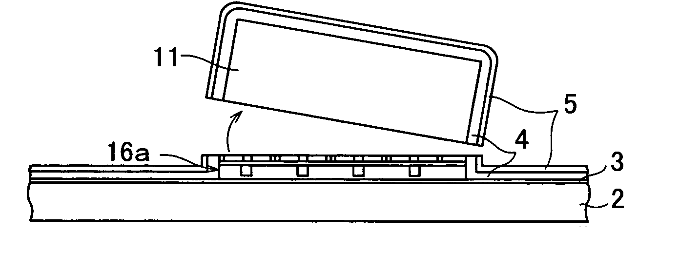
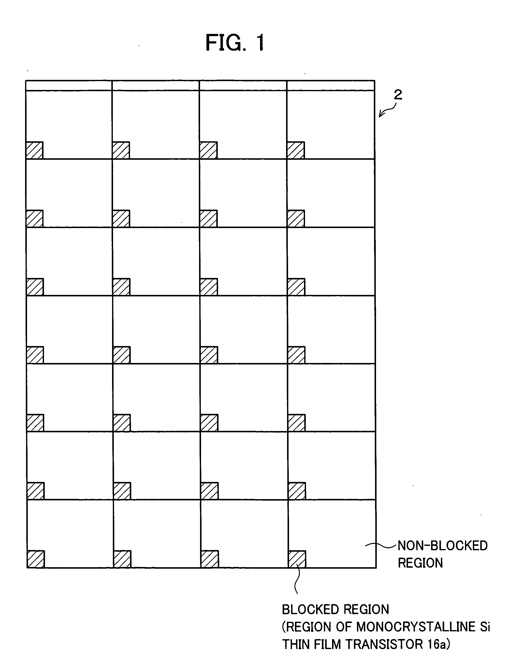
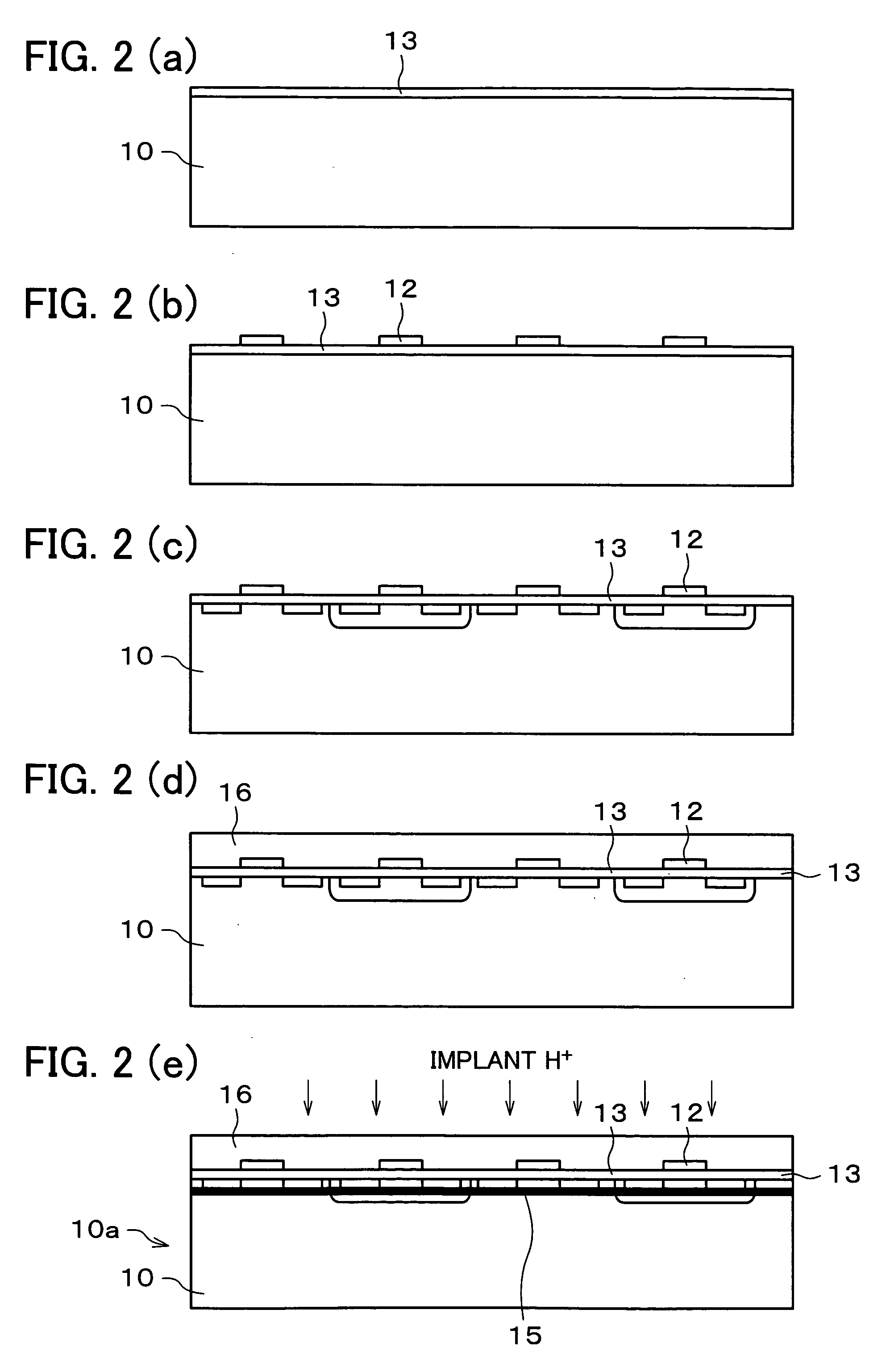
[0035] As described herein, a semiconductor device of the present embodiment provides improved performance and improved functionality by forming a MOS polycrystalline Si thin film transistor (deposited device, second device) and a MOS monocrystalline Si thin film transistor (transferred device, first device) in different regions on an insulating substrate. As described in this embodiment, the semiconductor device is formed on an active-matrix substrate using TFT.

[0036] The MOS thin film transistor is a common transistor including an active semiconductor layer, an gate electrode, a gate insulating film, and dense impurity doped portions (source electrodes and drain electrodes) formed on the both sides of a gate, wherein the gate electrode adjusts the carrier density of the semiconductor layer beneath the gate, so as to adjust a flow of source-drain curr...

second embodiment

[0104] [Second Embodiment]

[0105] Another embodiment of the present invention is described below with reference to the attached drawings. Note that, for convenience of explanation, members having the same functions are those described in conjunction with the semiconductor device of the foregoing First Embodiment are given the same reference numerals and detailed explanation thereof is omitted here.

[0106] As in the semiconductor device of the First Embodiment, a semiconductor device of the present embodiment provides improved performance and improved functionality by forming a MOS polycrystalline Si thin film transistor (deposited device, second device) and a MOS monocrystalline Si thin film transistor (transferred device, first device) in different regions on an insulating substrate. As described in this embodiment, the semiconductor device is formed on an active-matrix substrate using TFT.

[0107] As illustrated in FIG. 5(g), a semiconductor device 20 of the present embodiment inclu...


PUM


Abstract

An insulating substrate is bonded to a monocrystalline Si substrate that includes a monocrystalline Si thin film transistor and a hydrogen ion implanted portion. After depositing an amorphous Si thin film, the amorphous Si thin film is modified into a polycrystalline Si thin film by irradiation of the excimer laser. In laser irradiation, the irradiation of the laser beam on the monocrystalline Si thin film transistor is blocked either by inserting a mask in part of the optical path of the laser beam, or by irradiating the laser beam before unnecessary portions of the monocrystalline Si substrate is detached. In this way, the irradiation of the laser beam for forming the polycrystalline Si thin film will not damage the monocrystalline Si thin film transistor in a semiconductor device in which the monocrystalline Si thin film transistor, which has been transferred, and the polycrystalline Si thin film transistor, which has been formed on the insulating substrate, are formed on the insulating substrate.

Description

[0001] This Nonprovisional application claims priority under 35 U.S.C. § 119(a) on Patent Application No. 2003-206111 filed in Japan on Aug. 5, 2003, and No. 2003-308859 filed in Japan on Sep. 1, 2003, the entire contents of which are hereby incorporated by reference. FIELD OF THE INVENTION [0002] The present invention relates to a fabrication method of a semiconductor device with two kinds of transistors of different characteristics formed on a single substrate. Particularly, the invention relates to a semiconductor device fabrication method for improving circuit performance of a display device when a peripheral driving circuit and a control circuit are integrated on a single substrate in, for example, active-matrix liquid crystal display devices, active-matrix organic EL display devices and the like that employ TFT driving. BACKGROUND OF THE INVENTION [0003] With the recent pervasion of personal information terminals using a computer or flat display panel, there has been rapid dev...

Claims


Application Information

Patent Timeline
IPC IPC(8): H01L21/20H01L21/60H01L21/762H01L21/77H01L21/84H01L27/12
CPCH01L21/2026H01L2924/01033H01L21/84H01L24/18H01L24/82H01L27/12H01L27/1214H01L27/1266H01L2221/68359H01L2221/68368H01L2224/18H01L2924/01005H01L2924/01015H01L2924/01027H01L2924/01046H01L2924/01057H01L2924/01058H01L2924/01061H01L2924/01074H01L2924/01077H01L2924/01078H01L2924/01079H01L2924/01082H01L2924/01088H01L2924/01094H01L2924/13091H01L2924/14H01L2924/01006H01L2924/01021H01L2924/01023H01L21/76254H01L2924/12042H01L2224/92244H01L2224/32225H01L24/19H01L2224/04105H01L2224/73267H01L21/0262H01L21/02592H01L21/02686H01L21/02422H01L21/02678H01L21/02488H01L21/02532H01L21/02691H01L2924/00H01L21/20H01L21/02667
Inventor ITOGA, TAKASHITAKAFUJI, YUTAKAYAMAMOTO, YOSHIHIRO
Owner SHARP KK
Why Eureka
Try Eureka