Chip structure and process for forming the same

a technology of chip structure and process, applied in the direction of semiconductor devices, semiconductor/solid-state device details, inductance, etc., can solve the problems of noise, resistance-capacitor delay of key traces, voltage drop of buses, etc., to improve resistance-capacitance delay and reduce chip energy loss.

Inactive Publication Date: 2005-02-10
QUALCOMM INC +1
View PDF16 Cites 8 Cited by
  • Summary
  • Abstract
  • Description
  • Claims
  • Application Information

AI Technical Summary

Benefits of technology

Accordingly, an objective of the present invention is to provide a chip structure and a process for forming the same that improves resistance-capacitance delay and reduces energy loss of the chip.

Problems solved by technology

However, the relatively fine interconnections therein negatively impact the chip.
For example, this causes the voltage drop of the buses, the resistance-capacitor delay of the key traces, and noises, etc.
In particular, the RC delay even usually occurs with respect to a power bus, a ground bus or other metal lines transmitting common signals.
This causes production costs to dramatically rise.

Method used


Image

  • Chip structure and process for forming the same
  • Chip structure and process for forming the same
  • Chip structure and process for forming the same

Examples


first embodiment

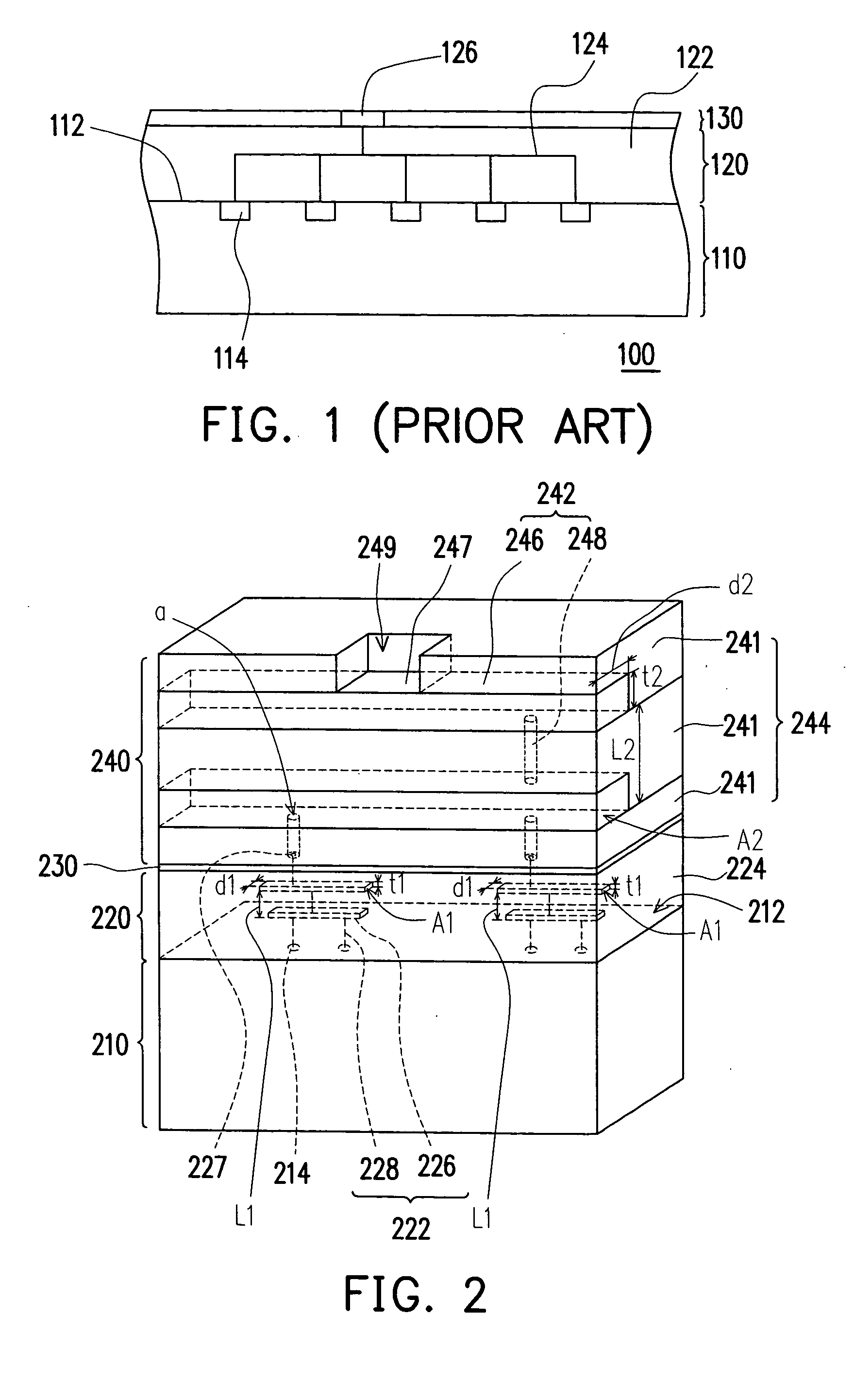
According to the above conception, the present invention provides various improved chip structure. Please refer to FIG. 2, a cross-sectional view schematically showing a chip structure according to the present invention. A chip structure 200 is provided with a substrate 210, a first built-up layer 220, a passivation layer 230 and a second built-up layer 240. There are plenty of electric devices 214, such as transistors, on a surface 212 of the substrate 210, wherein the substrate 210 is made of, for example, silicon. The first built-up layer 220 is located on the substrate 210. The first built-up layer 220 is formed by cross lamination of first metal multi-layers 226 and first dielectric multi-layers. Moreover, plugs 228 connect the upper first metal layers 226 with the lower first metal layers 226 or connect the first metal layers 226 with the electric devices 214. The first metal multi-layers 226 and the plugs 228 compose a first interconnection scheme 222. The first dielectric mu...

second embodiment

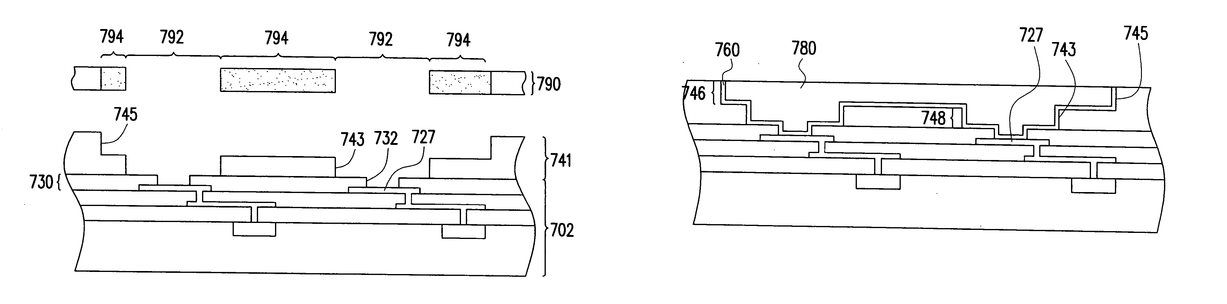
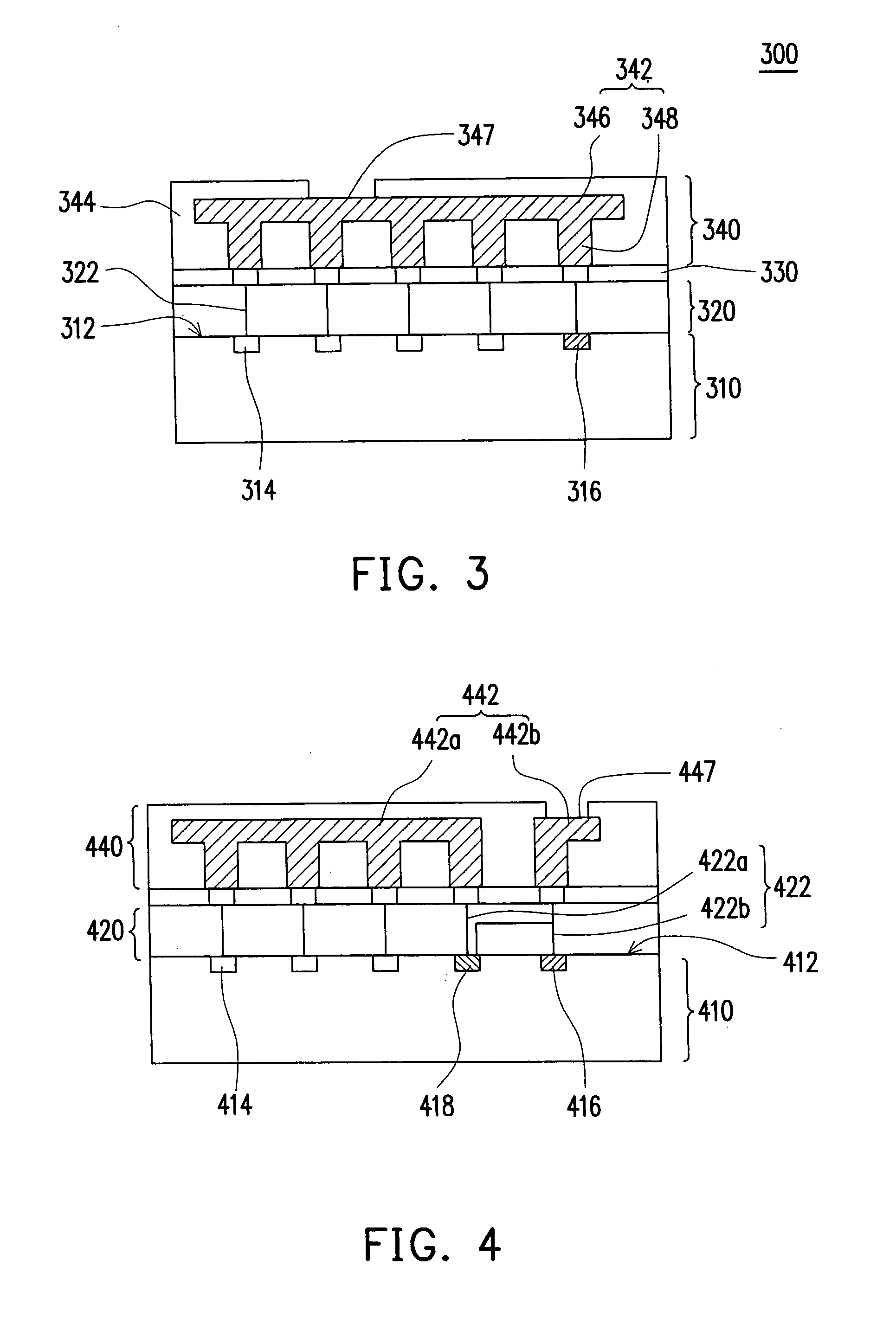
Next, other preferred embodiments of the present invention will be introduced. As a lot of electric devices are electrically connected with a power bus and a ground bus, the current through the power bus and the ground bus is relatively large. Therefore, the second interconnection scheme of the second built-up layer can be designed as a power bus or a ground bus, as shown in FIG. 3. FIG. 3 is a cross-sectional view schematically showing a chip structure according to the present invention. The first interconnection scheme 322 of the built-up layer 320 electrically connects the second interconnection scheme 342 of the built-up layer 340 with the electric devices 314 and at least one electrostatic discharge circuit 316, wherein the electrostatic discharge circuit 316 is disposed on the surface 312 of the substrate 310. As a result, provided that the second interconnection scheme 342 is designed as a power bus, the second interconnection scheme 342 electrically connects with the power e...

third embodiment

Referring to FIG. 4, FIG. 4 is a cross-sectional view schematically showing a chip structure according to the present invention. There are many electric devices 414, many electrostatic discharge circuits 416 (only shows one of them) and many transition devices 418 (only shows one of them) on the surface 412 of the substrate 410. The first interconnection scheme 422 is divided into first interconnections 422a and first transition interconnections 422b. The second interconnection scheme 442 is divided into second interconnections 442a and second transition interconnections 442b. Consequently, the nodes 447 are electrically connected with the transition devices 418 and the electrostatic discharge circuits 416 through the first transition interconnections 422b and the second transition interconnections 442b. The transition devices 418 are electrically connected with the electric devices 414 through the first interconnections 422a and the second interconnections 442a. For example, this c...


PUM


Abstract

A chip structure comprises a substrate, a first built-up layer, a passivation layer and a second built-up layer. The substrate includes many electric devices placed on a surface of the substrate. The first built-up layer is located on the substrate. The first built-up layer is provided with a first dielectric body and a first interconnection scheme, wherein the first interconnection scheme interlaces inside the first dielectric body and is electrically connected to the electric devices. The first interconnection scheme is constructed from first metal layers and plugs, wherein the neighboring first metal layers are electrically connected through the plugs. The passivation layer is disposed on the first built-up layer and is provided with openings exposing the first interconnection scheme. The second built-up layer is formed on the passivation layer. The second built-up layer is provided with a second dielectric body and a second interconnection scheme, wherein the second interconnection scheme interlaces inside the second dielectric body and is electrically connected to the first interconnection scheme. The second interconnection scheme is constructed from at least one second metal layer and at least one via metal filler, wherein the second metal layer is electrically connected to the via metal filler. The thickness, width, and cross-sectional area of the traces of the second metal layer are respectively larger than those of the first metal layers.

Description

BACKGROUND OF THE INVENTION 1. Field of the Invention The invention relates in general to a chip structure and a process for forming the same. More particularly, the invention relates to a chip structure for improving the resistance-capacitance delay and a forming process thereof. 2. Description of the Related Art Nowadays, electronic equipment are increasingly used to achieve many various tasks. With the development of electronics technology, miniaturization, multi-function task, and comfort of utilization are among the principle guidelines of electronic product manufacturers. More particularly in semiconductor manufacture process, the semiconductor units with 0.18 microns have been mass-produced. However, the relatively fine interconnections therein negatively impact the chip. For example, this causes the voltage drop of the buses, the resistance-capacitor delay of the key traces, and noises, etc. FIG. 1 is a cross-sectional view showing a conventional chip structure with inte...

Claims


Application Information

Patent Timeline
Patent Type & Authority Applications(United States)
IPC IPC(8): H01L21/02H01L21/768H01L23/522H01L23/528H01L23/532H01L23/60H01L27/06H01L27/08
CPCH01L21/768H01L21/76807H01L2924/0002H01L21/76838H01L23/5222H01L23/5223H01L23/5227H01L23/5228H01L23/5286H01L23/5329H01L23/60H01L27/0676H01L27/08H01L28/10H01L28/20H01L2924/15174H01L2924/00
Inventor LIN, MOU-SHIUNGLEE, JIN-YUANHUANG, CHING-CHENG
Owner QUALCOMM INC
Why Eureka
Try Eureka