Ultrasound transmit beamformer integrated circuit and method

a beamformer and ultrasonic technology, applied in the field of coherent ultrasound imaging systems, can solve the problems of insufficient hardware resources to optimize the characteristics of transmit waveforms, insufficient programmability of carrier frequency characteristics, and insufficient precision of transmit waveforms, so as to achieve the effect of reducing power consumption, reducing the cost of transmission, and maintaining programmability of carrier frequency

Active Publication Date: 2005-02-10
MICROCHIP TECH INC
View PDF14 Cites 44 Cited by
  • Summary
  • Abstract
  • Description
  • Claims
  • Application Information

AI Technical Summary

Benefits of technology

The general purpose of the invention, which will be described below in greater detail, is to provide a novel method of transmit beamforming that allows for compact analog implementation of complex digital algorithms without compromising their features.
Another purpose of th

Problems solved by technology

Although prior analog beamformers support different apodization and delay profiles, their precision is inherently limited.
Another problem with analog transmit beam formation is insufficient hardware resources to optimize the characteristics of transmit waveforms.
The waveform shape or envelope is essentially fixed and, therefore, not optimal.
Since there is a plurality of transmit channels, the manufacturing cost, power dissipation and space constraints per channel are quite tough.
The major prob

Method used


Image

  • Ultrasound transmit beamformer integrated circuit and method
  • Ultrasound transmit beamformer integrated circuit and method
  • Ultrasound transmit beamformer integrated circuit and method

Examples


second embodiment

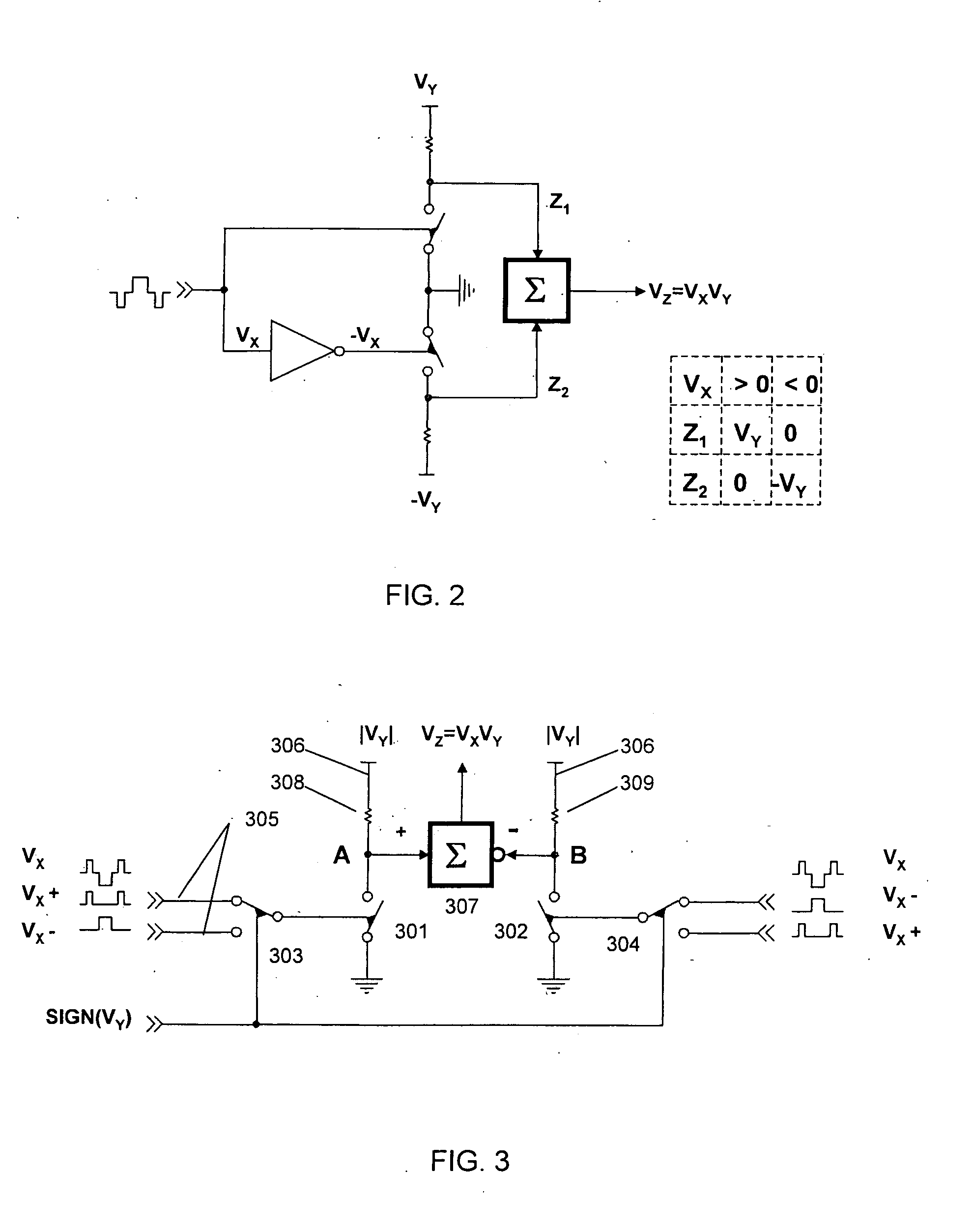
Since the gate voltage in FIG. 6 is formed as a product of phase rotating and apodization factors, it may have a wide dynamic range. Consequently, the threshold voltage tolerance of the transistor amplifiers may degrade the accuracy of beamformation. In view of that, the second embodiment shown in FIG. 5 introduces a different architecture.

FIG.5 depicts the second embodiment 500 comprises two identical pulse height and width multipliers 501, 520, a transmit controller 570, and an output multiplier 580. Each of the PHWMs 501 and 520 comprises two identical programmable current drivers 530, 540 and 550, 560. Interface and architecture of these drivers are shown in FIG. 7.

Referring to the PHWM 501, the first and second clock terminals 504, 506 of the first and the second drivers are connected in reverse. These terminals are fed by the PWM pulse train as discussed previously.

Switching inputs 508 of the first and second drivers 530, 540 are controlled by the polarity node 514. Refer...


PUM


Abstract

The invention provides a novel method of transmit beamforming, which allows compact analog implementation of complex digital algorithms without compromising their features. It is aimed to support envelope shaping, apodization, and phase rotation per channel and per firing. Each of three embodiments represents a complete transmit channel driven by pulse-width modulated (PWM) waveforms stored in a conventional sequence memory. PWM signals controls the transmit pulse envelope (shape) by changing the duty cycle of the carrier. Beamformation data are loaded prior to a firing via serial interface. Under the direction of a controller, the circuitry allows high precision (beyond sampling rate) phase rotation of the carrier. It also provides transmit apodization (aperture weighting), which maintains an optimal trade-off among low sidelobe level and widening of the mainlobe. Implementing such an IC, the manufacturing cost of a high-end ultrasound system can be reduced. Equally, the proposed solution makes the benefits of digital transmit beamformers available to midrange and entry-level machines since it merely requires a modified programming of the sequence memory.

Description

BACKGROUND OF THE INVENTION 1. Field of the Invention This invention relates to coherent ultrasound imaging systems and, in particular, phased array ultrasound imaging systems operating in different scan formats and imaging modes such as, B-, F-, M- and D- modes. Specifically, the invention relates to transmit beamforming and generating ultrasound transmit waveforms. 2. Background of the Invention An ultrasound scanner with an array transducer comprises a number of identical transmit and receive channels. Acting together, these channels produce transmit and receive beams, respectively. This process is referred as beamforming. It is accomplished by combining transmit / receive signals having variable delay and weight. There are two mainstream approaches in transmit beamforming: analog and digital. Although prior analog beamformers support different apodization and delay profiles, their precision is inherently limited. Another problem with analog transmit beam formation is insuffic...

Claims


Application Information

Patent Timeline
IPC IPC(8): G01S7/52G01S7/521G01S7/524G10K11/34H03F3/217
CPCG01S7/52017G01S7/52079G01S7/5202H03F3/217G10K11/34
Inventor SHIFRIN, LAZAR A.
Owner MICROCHIP TECH INC
Why Eureka
Try Eureka