Micromechanical device and method for producing a micromechanical device

a micromechanical and micro-mechanical technology, applied in the direction of fluid pressure measurement, acceleration measurement using interia forces, instruments, etc., can solve the problems of not being able to represent on one chip in a monolithically integrated manner, requiring multiple sensors, etc., to achieve cost-effective production, high sensitivity, cost-effective

Inactive Publication Date: 2007-06-07
ROBERT BOSCH GMBH
View PDF9 Cites 10 Cited by
  • Summary
  • Abstract
  • Description
  • Claims
  • Application Information

AI Technical Summary

Benefits of technology

[0008] According to the present invention, it may be provided that essentially a semiconductor material is provided as substrate material and/or that the spring pattern and the diaphragm pattern include essentially a monocrystalline material, e.g., monocrystalline silicon. This allows an especially cost-effective production of piezo-sensors which respond to even slight deflections of the diaphragm and the spring pattern, and thus operate with an especially high sensitivity.
[0009] The method according to the present invention has the advantage that the sensor patterns for the acceleration sensor and the pressure sensor are produced simultaneously, so that the production of the device according to the present invention is implementable in a particularly cost-effective manner. It is particularly advantageous that the seismic mass is made of substrate material, e.g., of semiconductor material. In the method according to the present invention, it may be provided that, for the application of the diaphragm patterning and the spring patterning into the substrate material, a partial area of the substrate material is etch

Problems solved by technology

In this context, it is disadvantageous that a plurality of sensors is required to measure several different mechanical variables, for instance to measure a pressure or an acceler

Method used


Image

  • Micromechanical device and method for producing a micromechanical device
  • Micromechanical device and method for producing a micromechanical device
  • Micromechanical device and method for producing a micromechanical device

Examples


Embodiment Construction

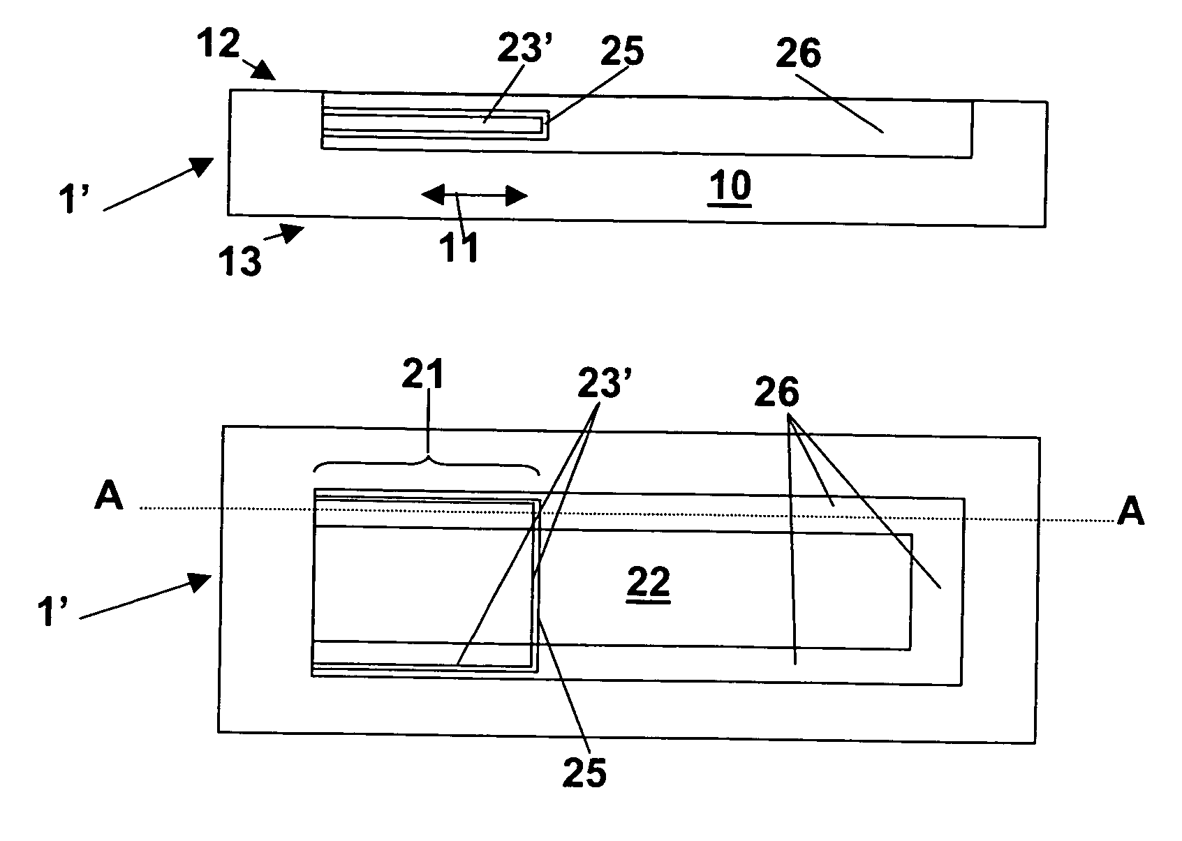
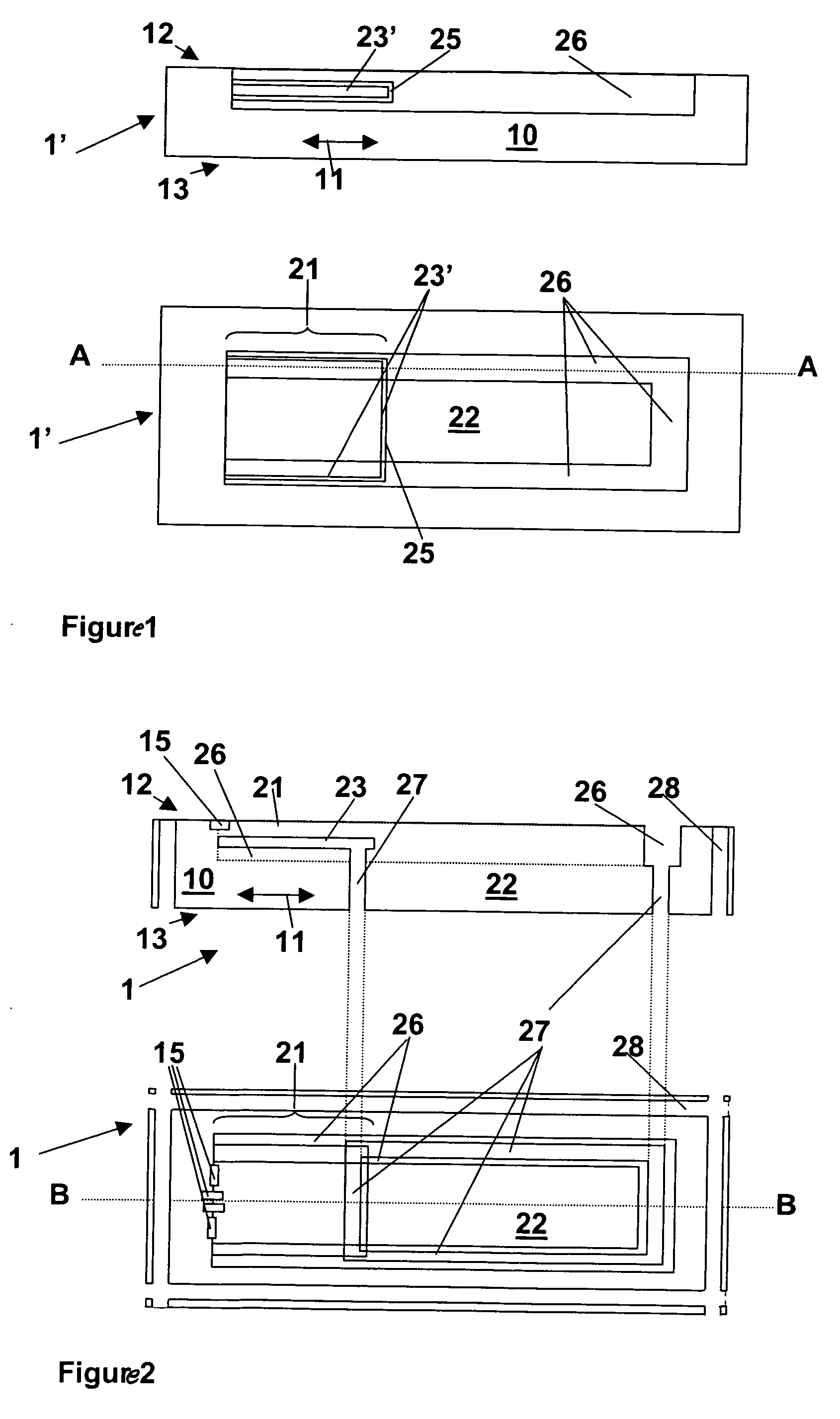
[0015]FIG. 1 shows a first precursor structure 1′ of the micromechanical device according to the present invention. FIG. 1 shows, in the lower part of FIG. 1, a top view having a sectional line A-A. In the upper part of FIG. 1, a sectional illustration of a section taken along sectional line A-A is shown. On a substrate material 10, which is provided as semiconductor material (e.g., a silicon wafer), and is therefore also designated as semiconductor material 10 in the following, a cavity 23′ is introduced as precursor of a clearance, described in greater detail below, under a spring pattern 21. Cavity 23′ is applied using the method steps of application of doping areas, subsequent porous etching and further subsequent thermal relocation. According to the present invention, semiconductor material 10 is a p-substrate, for instance, and the dopings introduced for the porous etching are negatively doped doping regions. Both the production of porous silicon regions using porous etching a...


PUM


Abstract

A micromechanical device and a method for producing this device are provided, the device having a sensor pattern that includes a spring pattern and a seismic mass. The seismic mass may be connected to the substrate material via the spring pattern, and a clearance may be provided in a direction perpendicular to the major substrate plane between the spring pattern and the substrate material. Alternatively, the spring pattern and the seismic mass may have a common, essentially continuous, front side surface.

Description

FIELD OF THE INVENTION [0001] The present invention relates to a micromechanical device configured as a sensor having a seismic mass. BACKGROUND INFORMATION [0002] A micromechanical device, e.g., a pressure sensor, is disclosed in published German patent document DE 103 23 559, in which pressure sensor the functionality of the sensor pattern is based on a piezoresistive converter principle for converting a mechanical force into an electrical signal. In this context, it is disadvantageous that a plurality of sensors is required to measure several different mechanical variables, for instance to measure a pressure or an acceleration, the sensors furthermore generally being based on different converter principles and therefore unable to be representable on one chip in a monolithically integrated manner. Applications in which simultaneous recording of a plurality of different mechanical variables, in particular pressure and acceleration, are desirable, are also found in the measurement o...

Claims


Application Information

Patent Timeline
IPC IPC(8): H01L29/82
CPCB81B3/0021B81B2201/0235B81B2201/0264G01L9/0042G01L19/0092G01P15/0802G01P15/0922
Inventor MUCHOW, JOERGBENZEL, HUBERTLANG, MARKUSGROTE, REGINAARMBRUSTER, SIMONLAMMEL, GERHARDSCHELLING, CHRISTOPHSENZ, VOLKMAR
Owner ROBERT BOSCH GMBH
Why Eureka
Try Eureka