Semiconductor device

a technology of semiconductor devices and barrier diodes, applied in the direction of transistors, basic electric elements, pulse automatic control, etc., to achieve the effect of enhancing the breakdown voltage of a schottky barrier diode, reducing the size of a semiconductor device, and ensuring design freedom

Inactive Publication Date: 2005-02-17
RENESAS ELECTRONICS CORP
View PDF3 Cites 19 Cited by
  • Summary
  • Abstract
  • Description
  • Claims
  • Application Information

AI Technical Summary

Benefits of technology

It is an object of the present invention to provide a technique capable of attaining the reduction in size of a semiconductor device which has a power transistor and a Schottky barrier diode on one and the same semiconductor substrate.
It is another object of the present invention to provide a technique capable of ensuring the freedom of design in a semiconductor device which has a power transistor and a Schottky barrier diode on one and the same semiconductor substrate.
It is a further object of the present invention to provide a technique capable of enhancing the breakdown voltage of a Schottky barrier diode in a semiconductor device which has a power transistor and the Schottky barrier diode on one and the same semiconductor substrate.
It is a still further object of the present invention to provide a technique capable of enhancing the breakdown voltage between source and drain of a power transistor in a semiconductor device which has the power transistor and a Schottky barrier diode on one and the same semiconductor device.

Problems solved by technology

However, having studied the semiconductor device with both a power MISFET of the trench gate structure and a Schottky barrier diode mounted on one and the same semiconductor substrate, the inventor in the present case found out the following problems.

Method used


Image

  • Semiconductor device
  • Semiconductor device
  • Semiconductor device

Examples


first embodiment

(First Embodiment)

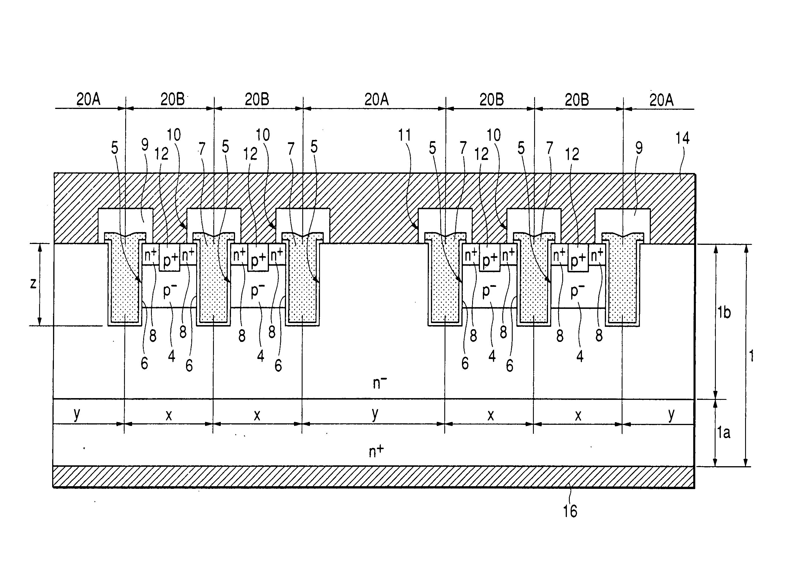
In this embodiment the present invention is applied to a semiconductor device which has a power MISFET of a trench gate structure and a Schottky barrier diode on one and the same semiconductor substrate.

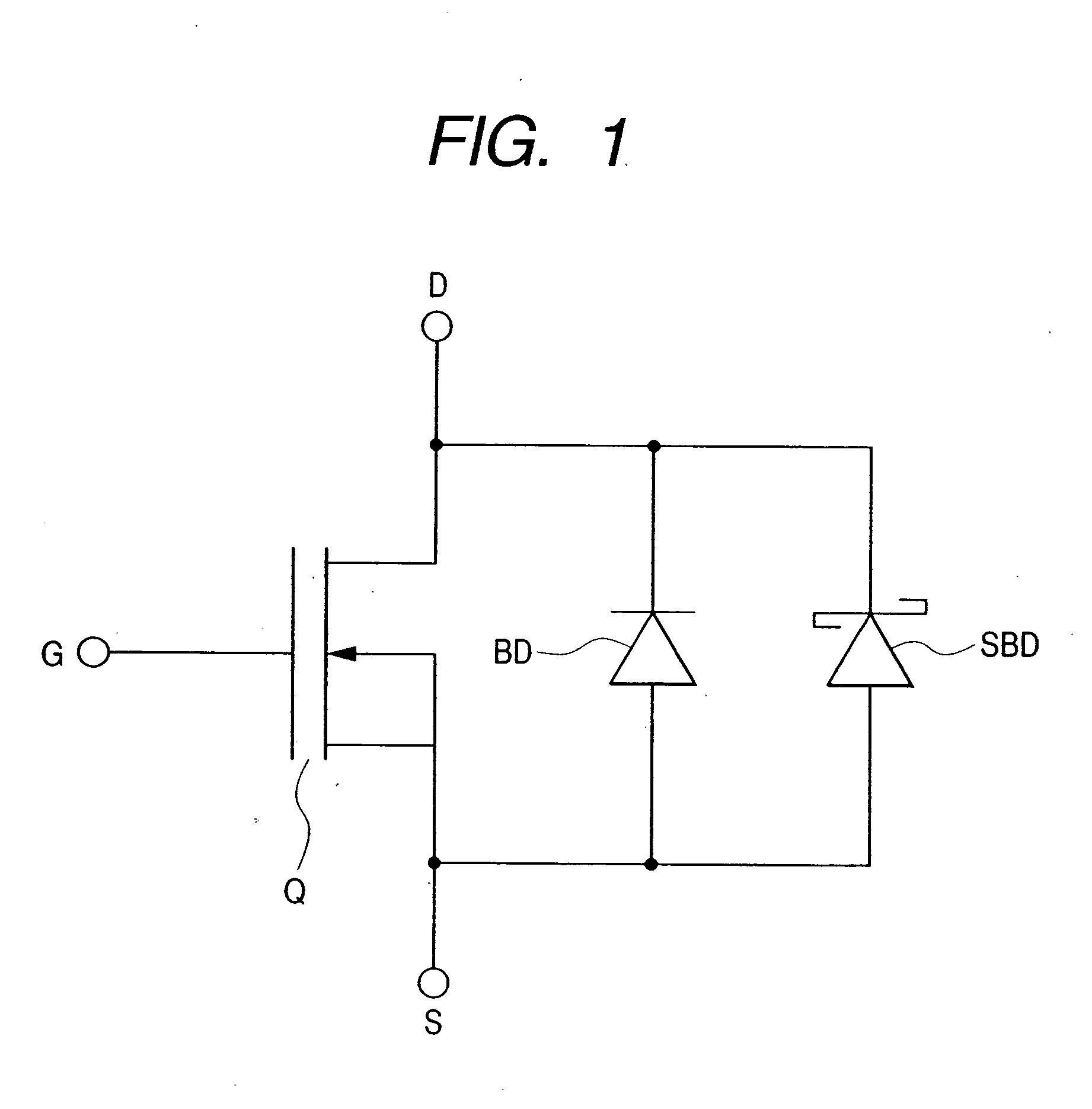
FIG. 1 is an equivalent circuit diagram of the semiconductor device of the first embodiment;

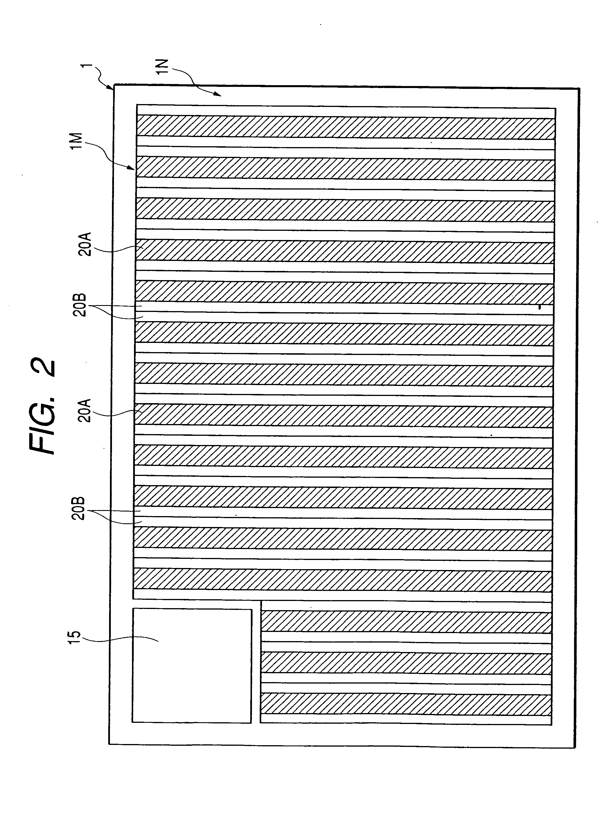
FIG. 2 is a chip layout diagram showing a schematic construction of the semiconductor device illustrated in FIG. 1;

FIG. 3 is a partially enlarged, schematic plan view of FIG. 2; and

FIG. 4 is a schematic sectional view taken along line A-A in FIG. 3.

As shown in FIG. 1, the semiconductor device of this embodiment has a power MISFET Q, a body diode BD, and a Schottky barrier diode SBD. These elements (Q, BD, SBD) are mounted on one and the same semiconductor substrate. The body diode BD and the Schottky barrier diode SBD are connected in parallel with the power MISFET Q. In the body diode BD and the Schottky barrier diode SBD, respective cathode regions are connected to a...

second embodiment

(Second Embodiment)

FIG. 5 is a chip layout diagram showing a schematic construction of a semiconductor device according to a second embodiment of the present invention;

FIG. 6 is an enlarged, schematic plan view of region C in FIG. 5;

FIG. 7 is an enlarged, schematic sectional view of region D in FIG. 5;

FIG. 8 is a schematic sectional view taken along line B-B in FIG. 5, with an intermediate portion omitted;

FIG. 9 is a schematic sectional view taken along line C-C in FIG. 5, with an intermediate portion omitted;

FIG. 10 is a partially enlarged, schematic sectional view of FIG. 8; and

FIG. 11 is a partially enlarged, schematic sectional view of FIG. 9.

The semiconductor device of this embodiment is basically of the same construction as the previous first embodiment and is different in the following constructional points from the first embodiment.

In the previous first embodiment plural Schottky cells 20A are connected in parallel to constitute one Schottky barrier diode SBD equiv...

third embodiment

(Third Embodiment)

FIG. 12 is a chip layout diagram showing a schematic construction of a semiconductor device according to a third embodiment of the present invention.

As shown in FIG. 12, the semiconductor device of this third embodiment is laid out so that a transistor device forming portion (active region) 2 with a transistor cell of power MISFET formed therein is surrounded by a Schottky device forming portion 21B with Schottky barrier diode SBD formed therein. Even with such a layout, the plane size (chip size) of the semiconductor substrate 1 can be made small as in the first embodiment. It is also possible to ensure the freedom in design of the semiconductor device.

Since the Schottky barrier diode is generally a surface device determined by the interface between metal and semiconductor, it is preferable that damage in package assembly (especially damage in wire bonding) be as small as possible. As in this third embodiment, by making layout so that the transistor device for...


PUM


Abstract

To attain reduction in size of a semiconductor device having a power transistor and an SBD, a semiconductor device according to the present invention comprises a first region and a second region formed on a main surface of a semiconductor substrate; plural first conductors and plural second conductors formed in the first and second regions respectively; a first semiconductor region and a second semiconductor region formed between adjacent first conductors in the first region, the second semiconductor region lying in the first semiconductor region and having a conductivity type opposite to that of the first semiconductor region; a third semiconductor region formed between adjacent second conductors in the second region, the third semiconductor region having the same conductivity type as that of the second semiconductor region and being lower in density than the second semiconductor region; a metal formed on the semiconductor substrate in the second region, the third semiconductor region having a metal contact region for contact with the metal, the metal being electrically connected to the second semiconductor region, and a center-to-center distance between adjacent first conductors in the first region being smaller than that between adjacent second conductors in the second region.

Description

BACKGROUND OF THE INVENTION The present invention relates to a semiconductor device and particularly to a technique which is effectively applicable to a semiconductor device having a power transistor and a Schottky barrier diode (SBD) on one and the same semiconductor substrate. As a semiconductor device used as a switching device in a power amplifier or a power supply circuit there is known, for example, a power transistor called power MISFET (Metal Insulator Semiconductor Field Effect Transistor). The power MISFET has a structure wherein plural transistor cells comprising fine patterns of MISFETs are connected in parallel to obtain a large power. Power MISFETs called vertical type and horizontal type are known. As to the vertical type, one called a trench gate structure is also known. MISFET indicates an insulated gate type field effect transistor wherein a gate insulating film (insulating film) is interposed between a channel forming region (semiconductor) and a gate electrode...

Claims


Application Information

Patent Timeline
Patent Type & Authority Applications(United States)
IPC IPC(8): H01L29/872H01L21/8234H01L27/04H01L27/088H01L27/095H01L29/06H01L29/08H01L29/10H01L29/40H01L29/45H01L29/47H01L29/78H01L31/0336H01L31/062
CPCH01L29/0615H01L29/475H01L29/0696H01L29/0847H01L29/0878H01L29/1095H01L29/402H01L29/407H01L29/456H01L29/47H01L29/7802H01L29/7806H01L29/7811H01L29/7813H01L29/782H01L29/7823H01L29/872H01L29/8725H01L27/0629H01L29/20H01L29/4236H01L29/0619H01L2224/0603
Inventor SHIRAI, NOBUYUKIMATSUURA, NOBUYOSHINAKAZAWA, YOSHITO
Owner RENESAS ELECTRONICS CORP
Why Eureka
Try Eureka