Scanning system for inspecting anamolies on surfaces

a scanning system and anamoly technology, applied in the field of surface inspection systems, can solve the problems of undetectable background, affecting the uniformity of the spot along the scan line, and reducing the size of the illuminated area, so as to reduce the size of the illuminated area and reduce the scattering of light. , the effect of reducing the size of the area

Inactive Publication Date: 2005-02-17
KLA TENCOR TECH CORP
View PDF91 Cites 1 Cited by
  • Summary
  • Abstract
  • Description
  • Claims
  • Application Information

AI Technical Summary

Benefits of technology

This invention is based on the recognition that very small anamolies can be detected by reducing the size of the area that is illuminated by the scanning light beam. Light scattered from structures in the spot will include background, such as light scattered by pattern on the surface, as well as light that is scattered by anomalies such as contaminant particles, pattern defects or imperfections of the surface. Such background can have a significant amplitude. For this reason, if the anamoly is of a size which is small compared to the size of the illuminated area, the scattered light from such anamoly may be overwhelmed by and become undetectable from the background. By reducing the size of the illuminated area or spot size, the ratio of the light intensity scattered by an anomaly to that of the background will be increased, thereby increasing detection sensitivity. However, with a smaller spot size, it will be more difficult to maintain the uniformity of the spot along a long straight scan line across the entire wafer. By breaking up the scan path into short segments, it is possible to employ a smaller spot size while at the same time maintaining uniformity of the spot along the path. From the system point of view, by reducing the length of the scan, the size of the collection optics for detecting forward scattered light becomes more manageable.

Problems solved by technology

For this reason, if the anamoly is of a size which is small compared to the size of the illuminated area, the scattered light from such anamoly may be overwhelmed by and become undetectable from the background.
However, with a smaller spot size, it will be more difficult to maintain the uniformity of the spot along a long straight scan line across the entire wafer.

Method used


Image

  • Scanning system for inspecting anamolies on surfaces
  • Scanning system for inspecting anamolies on surfaces
  • Scanning system for inspecting anamolies on surfaces

Examples


Embodiment Construction

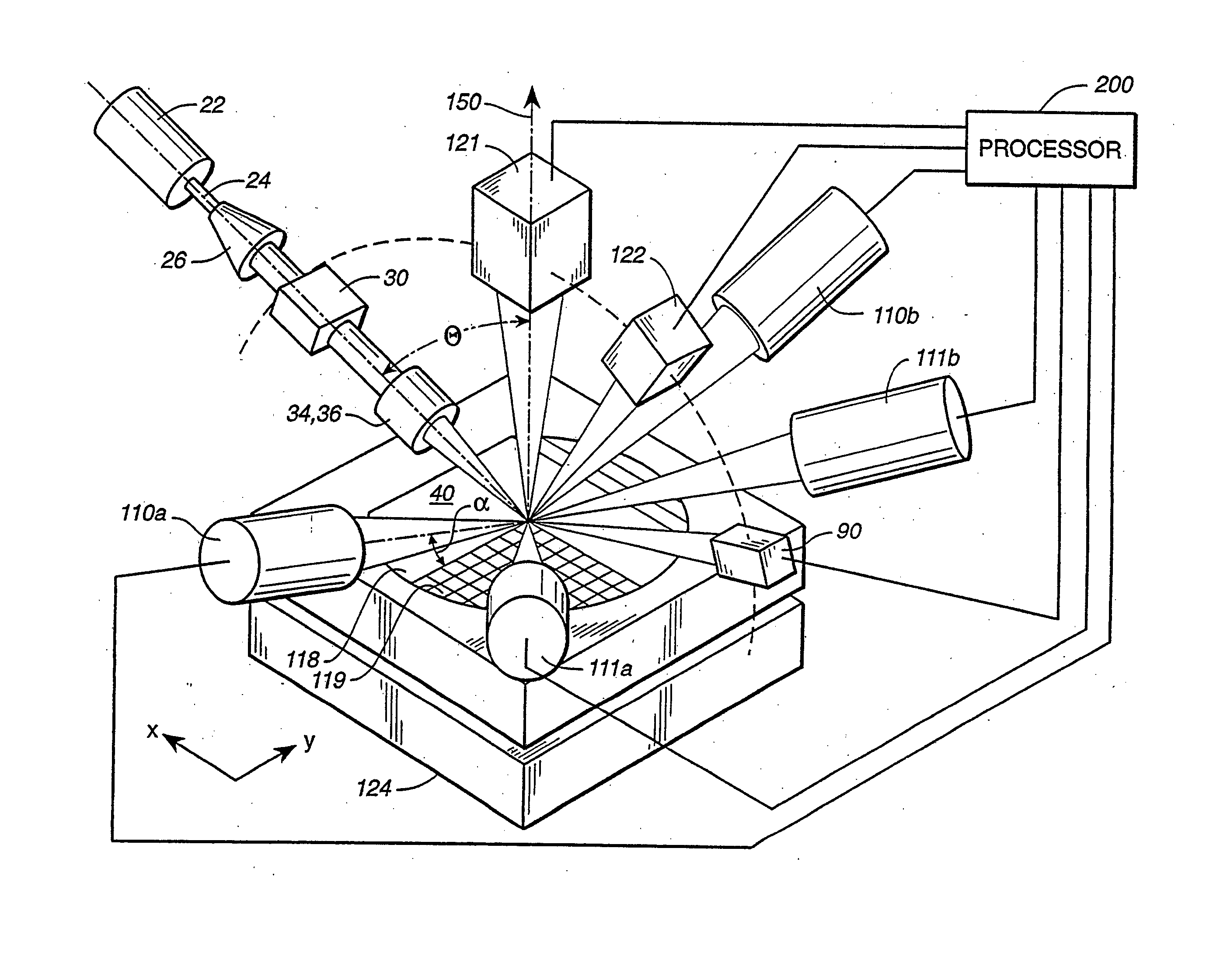
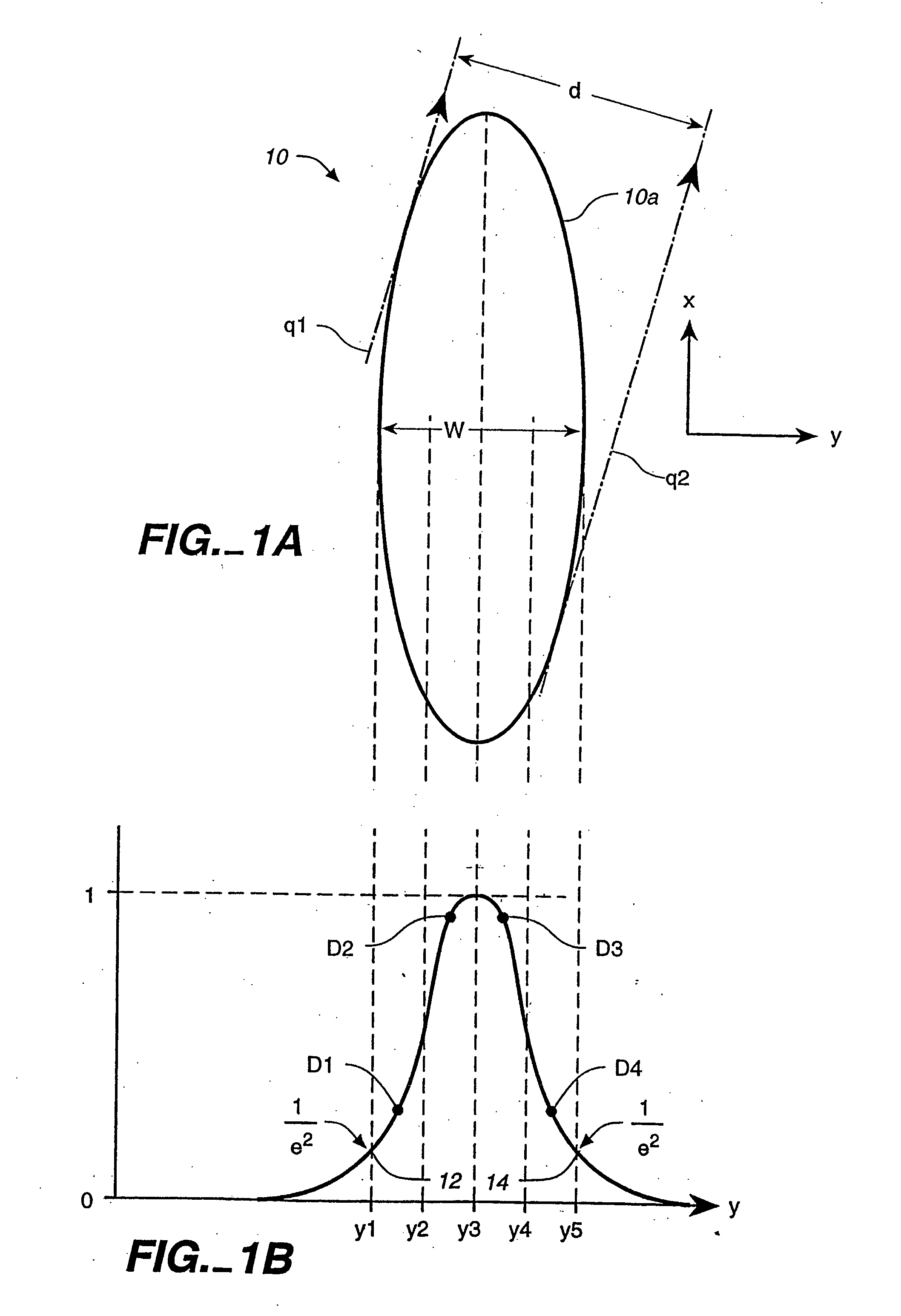
FIG. 1A is a schematic view of an elliptical-shaped illuminated area (or spot) of a surface inspected by the system of this invention to illustrate the invention. As explained below, the laser beam illuminating the surface inspected approach the surface at a grazing angle, so that even though the illumination beam has a generally circular cross-section, the area illuminated is elliptical in shape such as area 10 in FIG. 1A. As known to those skilled in the art, in light beams such as laser beams, the intensity of the light typically does not have a flat distribution and does not fall off abruptly to zero across the boundary of the spot illuminated, such as at boundary 10a of spot 10 of FIG. 1A. Instead, the intensity falls off at the outer edge of the illuminated spot at a certain inclined slope, so that instead of sharp boundaries such as boundary 10a illustrated in FIG. 1A, the boundary is typically blurred and forms a band of decreasing intensity at increasing distance away from ...


PUM

PropertyMeasurementUnit
widthaaaaaaaaaa
diameteraaaaaaaaaa
diameteraaaaaaaaaa

Abstract

A high sensitivity and high throughput surface inspection system directs a focused beam of light at a grazing angle towards the surface, to be inspected. Relative motion is caused between the beam and the surface so that the beam scans a scan path covering substantially the entire surface and light scattered along the path is collected for detecting anamolies. The scan path comprises a plurality of arrays of straight scan path segments. The focused beam of light illuminates an area of the surface between 5-15 microns in width and this system is capable of inspecting in excess of about 40 wafers per hour for 150 millimeter diameter wafers (6-inch wafers), in excess of about 20 wafers per hour for 200 millimeter diameter wafers (8-inch wafers) and in excess of about 10 wafers per hour for 300 millimeter diameter wafers (12-inch wafers).

Description

BACKGROUND OF THE INVENTION This invention relates in general to surface inspection systems, and in particular, to a high speed scanner system for inspecting anamolies on surfaces such as semiconductor wafers, photomasks, reticles, ceramic tiles, and other surfaces. The size of semiconductor devices fabricated on silicon wafers has been continually reduced. At the time this application is filed, for example, semiconductor devices can be fabricated at a resolution of a half micron or less and sixty-four (64) megabyte DRAMS are being fabricated with 0.35 micron design rule. The shrinking of semiconductor devices to smaller and smaller sizes has imposed a much more stringent requirement for sensitivity of wafer inspection instruments which are called upon to detect contaminant particles and pattern defects that are small compared to the size of the semiconductor devices. On the other hand, it is desirable for wafer inspection systems to provide an adequate throughput so that these sy...

Claims


Application Information

Patent Timeline
Patent Type & Authority Applications(United States)
IPC IPC(8): G01N21/94G01N21/95G01N21/956
CPCG01N21/94G01N21/956G01N21/9501
Inventor NIKOONAHAD, MEHRDADSTOKOWSKI, STANLEY E.
Owner KLA TENCOR TECH CORP
Why Eureka
Try Eureka