Nitride semiconductor substrate production method thereof and semiconductor optical device using the same

a technology of nitride semiconductor substrate and production method, which is applied in the direction of sustainable manufacturing/processing, polycrystalline material growth, and final product manufacturing, etc., can solve the problems of cracking in the algan cladding layer, method using conventional dislocation-reducing technique, and difficulty in applications

Inactive Publication Date: 2005-02-17
MEIJO UNIVERSITY
View PDF2 Cites 53 Cited by
  • Summary
  • Abstract
  • Description
  • Claims
  • Application Information

AI Technical Summary

Benefits of technology

[0019] The present invention is directed to selectively grow a seed crystal made of GaN, or AlGaN having a relatively low AlN molar fraction, on a group-III nitride semiconductor, such as GaN, to have a specific crystal face, and then grow an AlGaN layer having a high AlN molar fraction through a group-III semiconductor, such as AIN deposited at a low temperature, so as to provide an AlGaN-crystal substrate having a low dislocation area in a wide range without any crack, and a high-performance optical device.
[0030] The intermediate layer is deposited at a low temperature of 300 to 800° C. If the temperature is greater than 800° C., the intermediate layer will be formed as a single crystal, and the lattice strain between the seed crystals, such as GaN, and the second semiconductor layer, such as AlGaN, formed on the intermediate layer will cause a crack in the second semiconductor layer etc. If the temperature is less than 800° C., no layer will be deposited due to thermal decomposition of a source gas. The intermediate layer deposited in the range of 300 to 800° C. is an aggregate of fine granular crystals which have a function of relaxing the stress due to the lattice mismatching to prevent the occurrence of crack.

Problems solved by technology

Methods using the conventional dislocation-reducing technique have difficulties in applications to light-emitting devices to be operated in a short wavelength range of 370 nm or less.
However, in the process of growing such an AlGaN cladding layer having a high AlN molar fraction on a GaN layer, a crack occurs in the AlGaN cladding layer.
Thus, the conventional methods cannot achieve the formation of a high-quality crystal having a low threading dislocation density without any crack.

Method used


Image

  • Nitride semiconductor substrate production method thereof and semiconductor optical device using the same
  • Nitride semiconductor substrate production method thereof and semiconductor optical device using the same
  • Nitride semiconductor substrate production method thereof and semiconductor optical device using the same

Examples


example

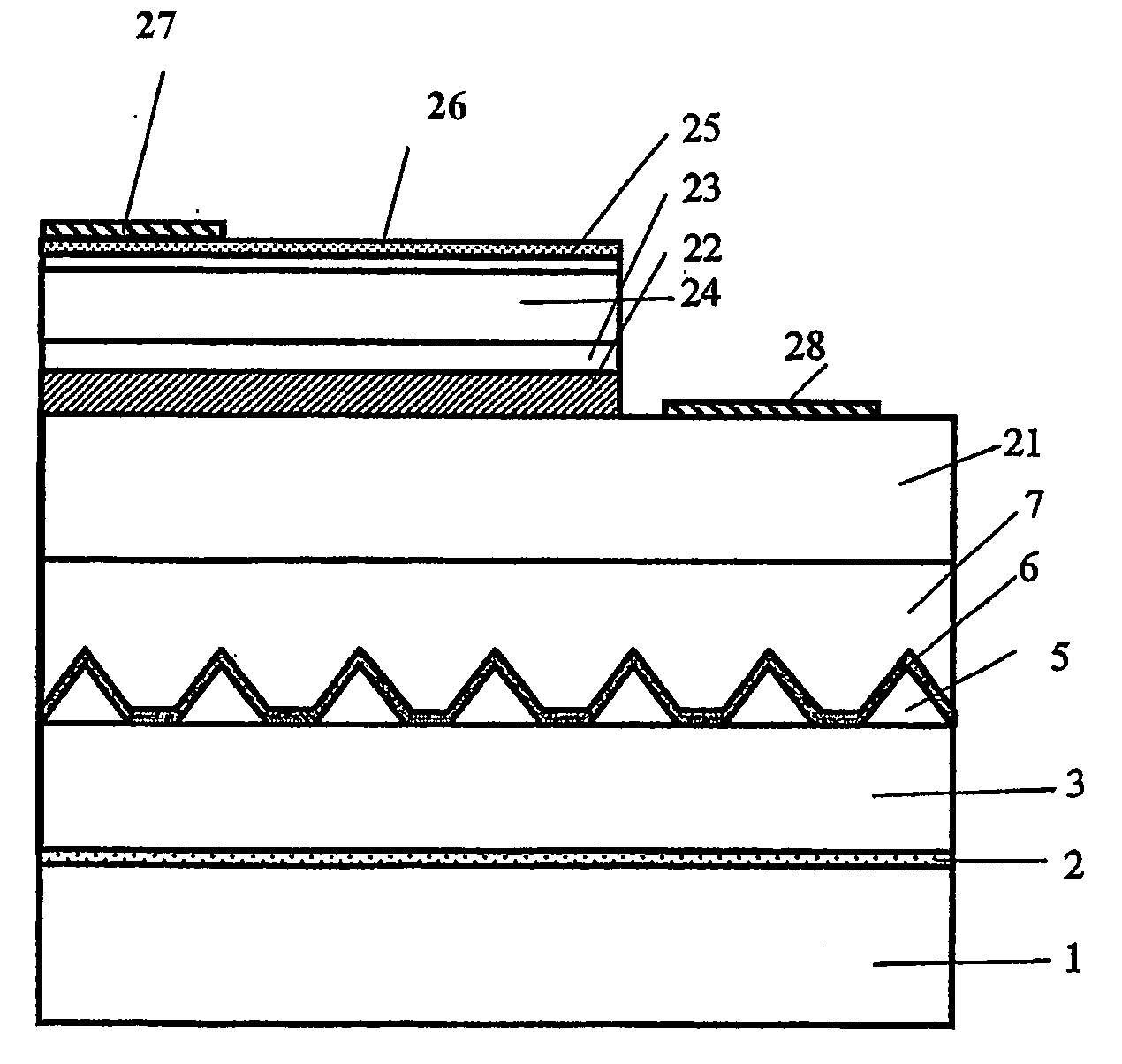
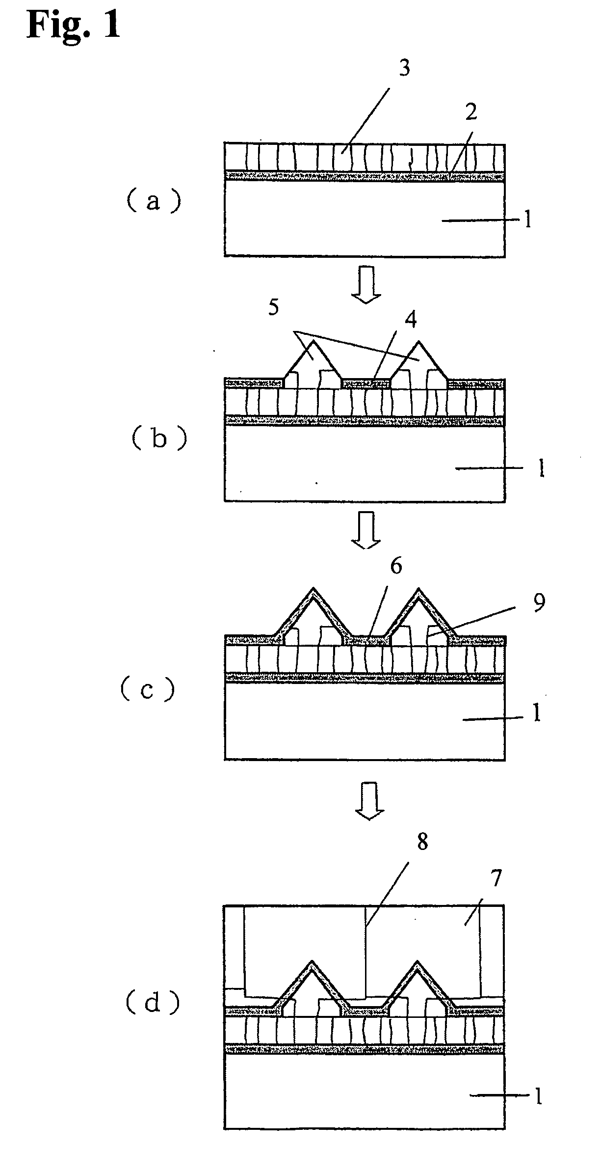
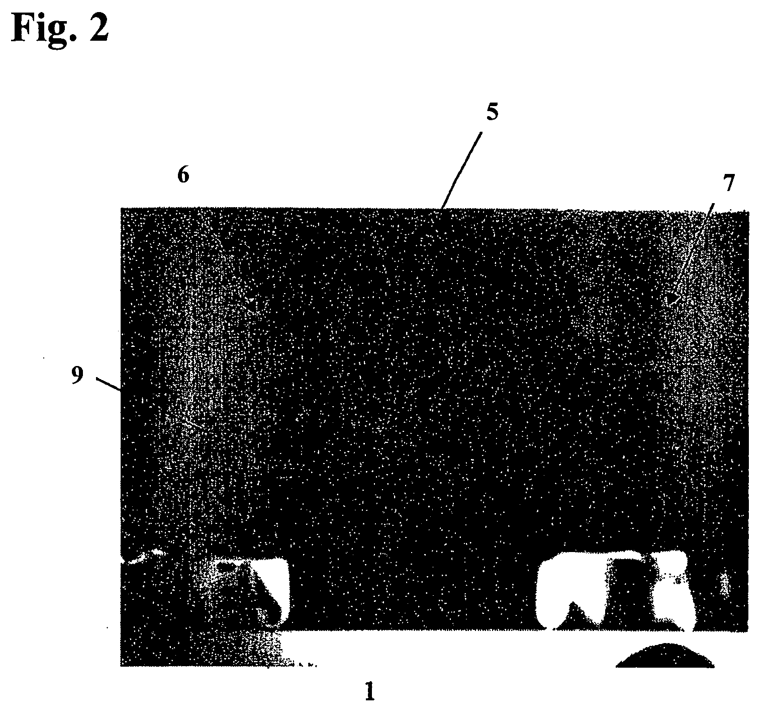
[0071] Based on the structure of the device according to the third embodiment, an ultraviolet light-emitting diode was produced. On the low-dislocation-density nitride semiconductor substrate illustrated in FIG. 1, an n-AI0.2Ga0.8N first cladding layer 21, a multi-quantum-well active layer 22, a p-Al0.4Ga0.6N cap layer 23, a p-Al0.2Ga0.8N second cladding layer 24, and a p-GaN contact layer 25 were successively grown in this order, through an organometallic-compound vapor phase growth. The multi-quantum-well active layer 22 was composed of a GaN quantum layer and an Al0.1Ga0.9N barrier layer, and the thickness of the GaN quantum layer was adjusted to be varied in the range of 2 nm to 4 nm to change the emission wavelength in the range of 320 nm to 360 nm. After the completion of the crystal growth, an ohmic semitransparent electrode 26 and a bonding pad electrode 27 each formed of a metal thin film were formed on the surface of the p-GaN contact layer 25, and an n-type electrode 28 w...


PUM

PropertyMeasurementUnit
wavelengthaaaaaaaaaa
temperatureaaaaaaaaaa
external quantum efficiencyaaaaaaaaaa

Abstract

Disclosed are a nitride semiconductor substrate and a production method thereof. Seed crystals made of GaN or AlGaN with a relatively low AIN molar fraction is selectively grown on a first group-III nitride semiconductor, such as GaN, to have a specific crystal face. Then, on the seed crystals, an AlGaN with a high AIN molar fraction is grown through a second group-III nitride semiconductor, such as AIN deposited at a low temperature. The present invention can provide an AlGaN-crystal substrate having a low dislocation density in a wide area without any crack, and a high-performance short-wavelength optical device using the substrate.

Description

TECHNICAL FIELD [0001] The present invention relates to the structure and production method of a group-III nitride semiconductor substrate which is expected to be applied, particularly, in the field of optical information processing. The present invention also relates to an optical semiconductor device formed using such a substrate. BACKGROUND ART [0002] Heretofore, there has been known light-emitting and light-receiving devices with a multilayered structure having a base layer made of group-III nitride semiconductor based on GaN or AlGaN with a relatively low molar fraction of AIN (see, for example, the after-mentioned Patent Publication 1 or Non-Patent Publication 1). FIG. 8 shows the structure of crystal layers in a typical conventional GaN-based light-emitting diode. This light-emitting diode includes n-GaN layer 103, an n-GaN first cladding layer 104, a GaInN / GaN multi-quantum-well active layer 105, a p-AlGaN cap layer 106, a p-GaN second cladding layer 107 and a p-GaN contact ...

Claims


Application Information

Patent Timeline
Patent Type & Authority Applications(United States)
IPC IPC(8): C30B25/02C30B25/18C30B29/40H01L21/20H01L21/205H01L31/0304H01L31/108H01L33/06H01L33/32H01L33/34
CPCC30B25/02Y02E10/544C30B29/403C30B29/406H01L21/0237H01L21/0242H01L21/02458H01L21/02502H01L21/02516H01L21/0254H01L21/02636H01L21/02658H01L31/03046H01L31/108H01L33/24H01L33/32C30B25/18Y02P70/50
Inventor KAMIYAMA, SATOSHIAMANO, HIROSHI
Owner MEIJO UNIVERSITY
Why Eureka
Try Eureka