Method for manufacturing nitride light-emitting device

Inactive Publication Date: 2005-02-24
FORMOSA EPITAXY INCORPORATION
View PDF7 Cites 14 Cited by
  • Summary
  • Abstract
  • Description
  • Claims
  • Application Information

AI Technical Summary

Benefits of technology

[0006] The primary object of the present invention is, on the one hand, to form an epitaxial layer of a nitride lighting structure on a high thermal conductivity substrate and prepare a vertical single lead wire structure, an N-type or P-type electrode for example, to hence lessen the light-shading area. On the other hand, an ohmic contact layer is formed to connect a transparent conductive layer with the N-type nitride epitaxial layer to have current di

Problems solved by technology

However, the effective lighting area of epitaxial grains has been lessened because both the P- and the N-type electrodes are inevitably arranged on the same side due to the insulating property of the substrate itself.
Because the conductivi

Method used


Image

  • Method for manufacturing nitride light-emitting device
  • Method for manufacturing nitride light-emitting device
  • Method for manufacturing nitride light-emitting device

Examples


Embodiment Construction

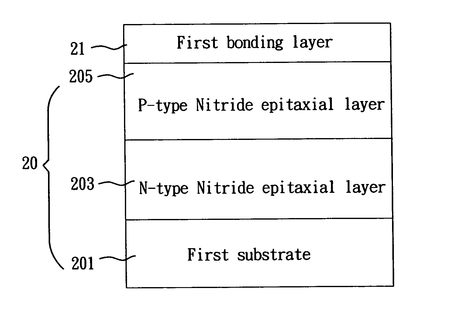
[0018]FIG. 1 shows a schematic lighting structure of nitride according to a method for manufacturing nitride light-emitting device of the present invention. As shown in FIG. 1, a lighting structure 20 according to a method for manufacturing nitride light-emitting device of the present invention comprises: a first substrate 201 made of aluminum oxide (Al2O3); an N-type nitride epitaxial layer 203, which is an epitaxial structure layer formed on the first substrate 201 by way of currently known epitaxial growth technology; and a P-type nitride epitaxial layer 205, which is also an epitaxial structure layer formed on the N-type nitride epitaxial layer 203 by the same technology growing the N-type nitride epitaxial layer 203.

[0019] For a bonding operation to be performed later, a first bonding layer 21 is grown on the P-type nitride epitaxial layer 205 of the nitride lighting structure 20 by depositing, sputtering, electroplating or other known techniques. In this case, depositing is a...


PUM

PropertyMeasurementUnit
Temperatureaaaaaaaaaa
Thicknessaaaaaaaaaa
Poweraaaaaaaaaa

Abstract

A method for manufacturing nitride light-emitting device is disclosed, which fixes two metallic bonding layers together in order to bond a nitride lighting structure grown on a poor thermal conductivity substrate to a high thermal conductivity substrate, then removes the poor thermal conductivity substrate by means of chemical etching, dry etching, or mechanical abrading to thereby transfer the nitride lighting structure onto that high thermal conductivity substrate. Meanwhile, by taking advantage of forming ohmic contact between a transparent conductive layer and an N-type nitride epitaxial layer, the uniformity of current distribution can be significantly improved to thereby suppress light absorption effect and heighten the lighting efficiency of the light emitting device.

Description

BACKGROUND OF THE INVENTION [0001] 1. Field of the Invention [0002] The present invention relates to a method for manufacturing nitride light-emitting device, and particularly to a manufacture method, which is to lay a light-emitting structure of nitride on a high thermal conductivity substrate by transference due to the formation of a bonding layer. [0003] 2. The Prior Arts [0004] An aluminum oxide (Al2O3) substrate is generally used in a common manufacture method of the prior nitride light-emitting device for growing epitaxy thereon. However, the effective lighting area of epitaxial grains has been lessened because both the P- and the N-type electrodes are inevitably arranged on the same side due to the insulating property of the substrate itself. Because the conductivity of the P-type nitride is far lower than that of the N-type, a translucent metallic conductive layer is adopted to serve for an ohmic contact layer for distributing current uniformly, which reduces light emitting ...

Claims


Application Information

Patent Timeline
IPC IPC(8): B23K31/02H01L33/00
CPCH01L33/0079H01L33/0093
Inventor YANG, KUANG-NENG
Owner FORMOSA EPITAXY INCORPORATION
Why Eureka
Try Eureka