

Horizontal current bipolar transistor and fabrication method
a bipolar transistor and horizontal current technology, applied in the field of bipolar transistor structures, can solve the problems of inferior high-frequency characteristics of the transistor compared to the state-of-art silicon substrate device, inferior electrical characteristics of the lateral pnp transistor compared to the mainstream npn transistor, and poor electrical characteristics of the cmos-based technology, so as to reduce the size of the integrated circuit die, reduce the area of the chip surface, and improve the effect of lateral pnp
- Summary
- Abstract
- Description
- Claims
- Application Information
AI Technical Summary
Benefits of technology
Problems solved by technology
Method used
Image

Examples
Embodiment Construction
[0023] Referring more specifically to the drawings, for illustrative purposes the present invention is embodied in the apparatus and methods generally shown and described in FIG. 1 through FIG. 6. It will be appreciated that the apparatus may vary as to configuration and as to details of the parts, and that the method may vary as to the specific steps and their sequence, without departing from the basic concepts as disclosed herein.
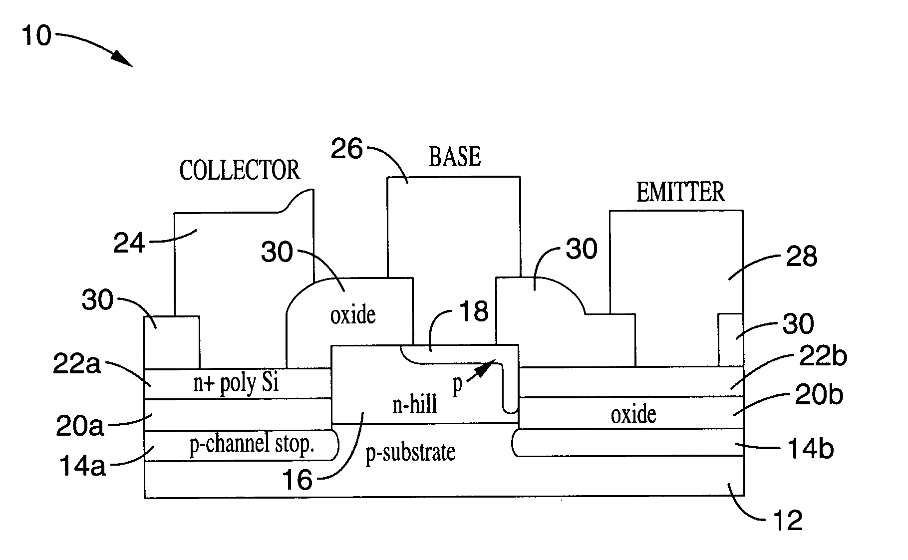
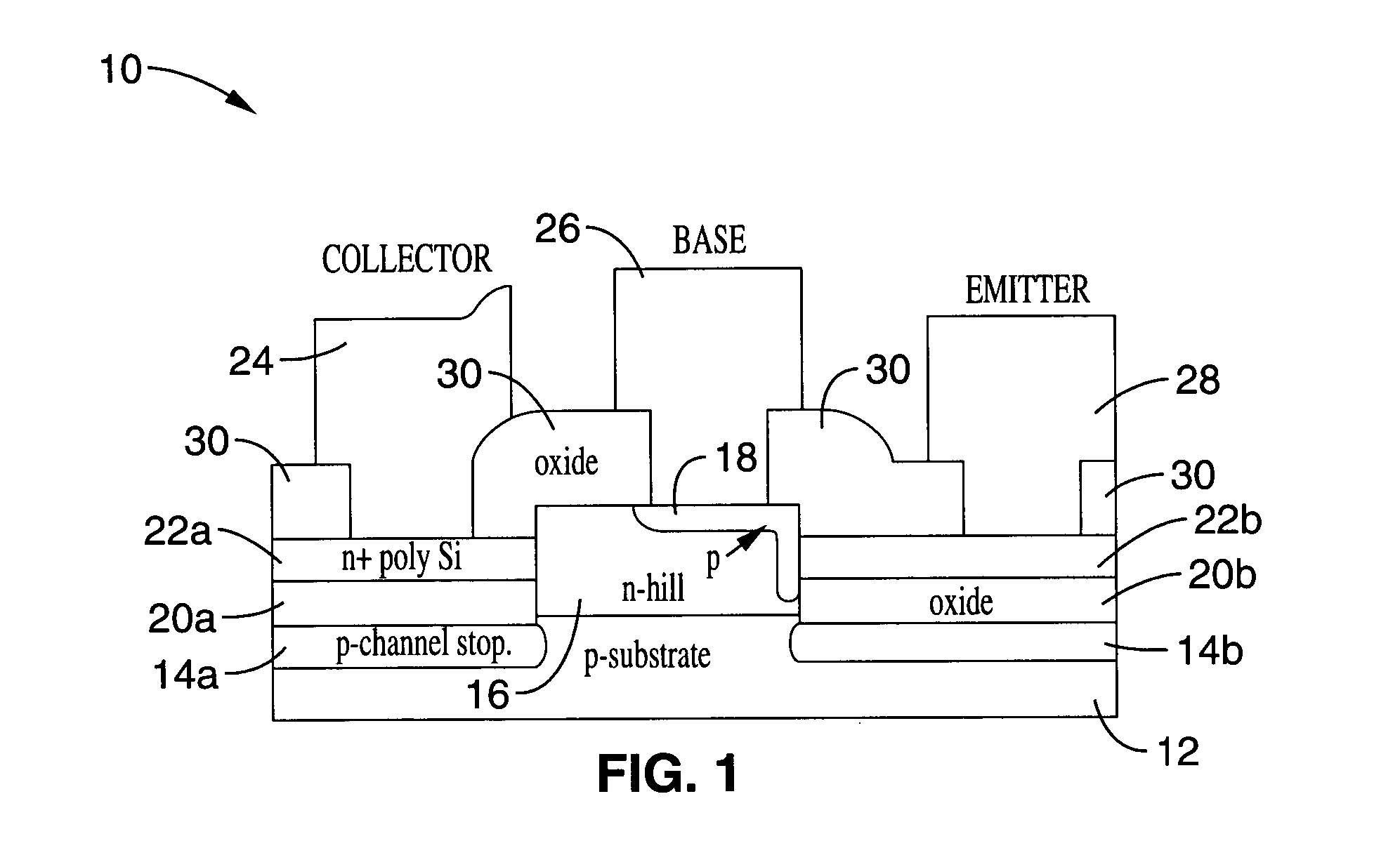
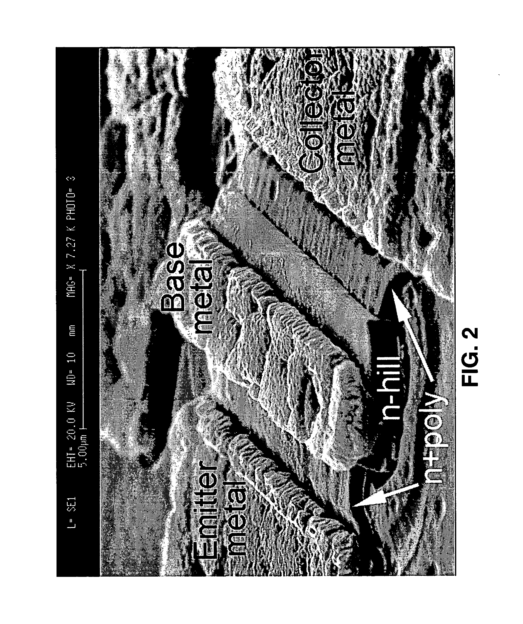
[0024] Referring first to FIG. 1, an embodiment of a Horizontal Current Bipolar Transistor (HCBT) 10 according to the present invention is schematically shown. In the embodiment shown, the device comprises p-type substrate 12, p-channel stoppers 14a, 14b, n-hill 16 with p-region 18, isolation silicon dioxide 20a, 20b, n+ polysilicon 22a, 22b, collector 24, base 26, emitter 28, and surrounding passivation oxide 30. FIG. 2 shows an SEM picture of such an HCBT in 1 μm lithography resolution and provides a perspective view of the device with the passivation ...
PUM
 Abstract
Description
Claims
Application Information