
Array substrate for a liquid crystal display device having an improved contact property and fabricating method thereof

a liquid crystal display and substrate technology, applied in semiconductor devices, instruments, optics, etc., can solve the problems of poor adhesion of cu to glass substrates, inferiority of electric signal inputs, and high diffusivity, so as to improve the electric characteristics of liquid crystal display devices, improve the contact property and fabricating methods, and improve the effect of electric characteristics

Inactive Publication Date: 2005-02-24
LG DISPLAY CO LTD
View PDF2 Cites 40 Cited by
  • Summary
  • Abstract
  • Description
  • Claims
  • Application Information

AI Technical Summary

Benefits of technology

[0017] An advantage of the present invention is to provide an array substrate for a liquid crystal display device having an improved contact property and fabricating method thereof.
[0018] An advantage of the present invention is to improve electric characteristics of a liquid crystal display device.
[0019] An advantage of the present invention is to provide an array substrate for a liquid crystal display device of a high aperture ratio using a copper line including a barrier layer where an inferior contact property due to an organic residue during a contact hole process is improved and electric characteristics increase through an effective combination of an organic insulating layer for high aperture ratio and a copper layer of low resistance.
[0020] Another advantage of the present invention is to provide an array substrate for a liquid crystal display device of a high aperture ratio using a copper line including a barrier layer where an upper copper layer is eliminated during a contact hole process and a lower barrier layer is electrically connected to an ITO layer.
[0021] Additional features and advantages of the invention will be set forth in the description that follows, and in part will be apparent from the description, or may be learned by practice of the invention. Other advantages of the invention will be realized and attained by the structure particularly pointed out in the written description and claims hereof as well as the appended drawings.
[0022] To achieve these and other advantages and in accordance with the purpose of the present invention, as embodied and broadly described, an array substrate for a liquid crystal display device includes: a substrate; a gate electrode on the substrate; a gate insulating layer on the gate electrode; a semiconductor layer on the gate insulating layer; source and drain electrodes on the semiconductor layer, the source and drain electrodes including a copper layer as an upper layer and a barrier layer as a lower layer; a first passivation layer on the source and drain electrodes; a second passivation layer on the first passivation layer, the second passivation layer having a drain contact hole through the first passivation layer, the drain contact hole exposing the barrier layer; and a pixel electrode connected to the barrier layer through the drain contact hole.

Problems solved by technology

However, since Cu has a poor adhesion to a glass substrate and a high diffusivity into a silicon material (e.g., insulating layer or semiconductor layer) under a relatively low temperature (about 200° C.
As a result, the organic residue 15 interferes an electric connection between the ITO layer and the Cu layer to cause an inferiority of electric signal input.

Method used


Image

  • Array substrate for a liquid crystal display device having an improved contact property and fabricating method thereof
  • Array substrate for a liquid crystal display device having an improved contact property and fabricating method thereof
  • Array substrate for a liquid crystal display device having an improved contact property and fabricating method thereof

Examples


Embodiment Construction

[0032] Reference will now be made in detail to the illustrated embodiments of the present invention, examples of which are illustrated in the accompanying drawings. Wherever possible, similar reference numbers will be used throughout the drawings to refer to the same or like parts.

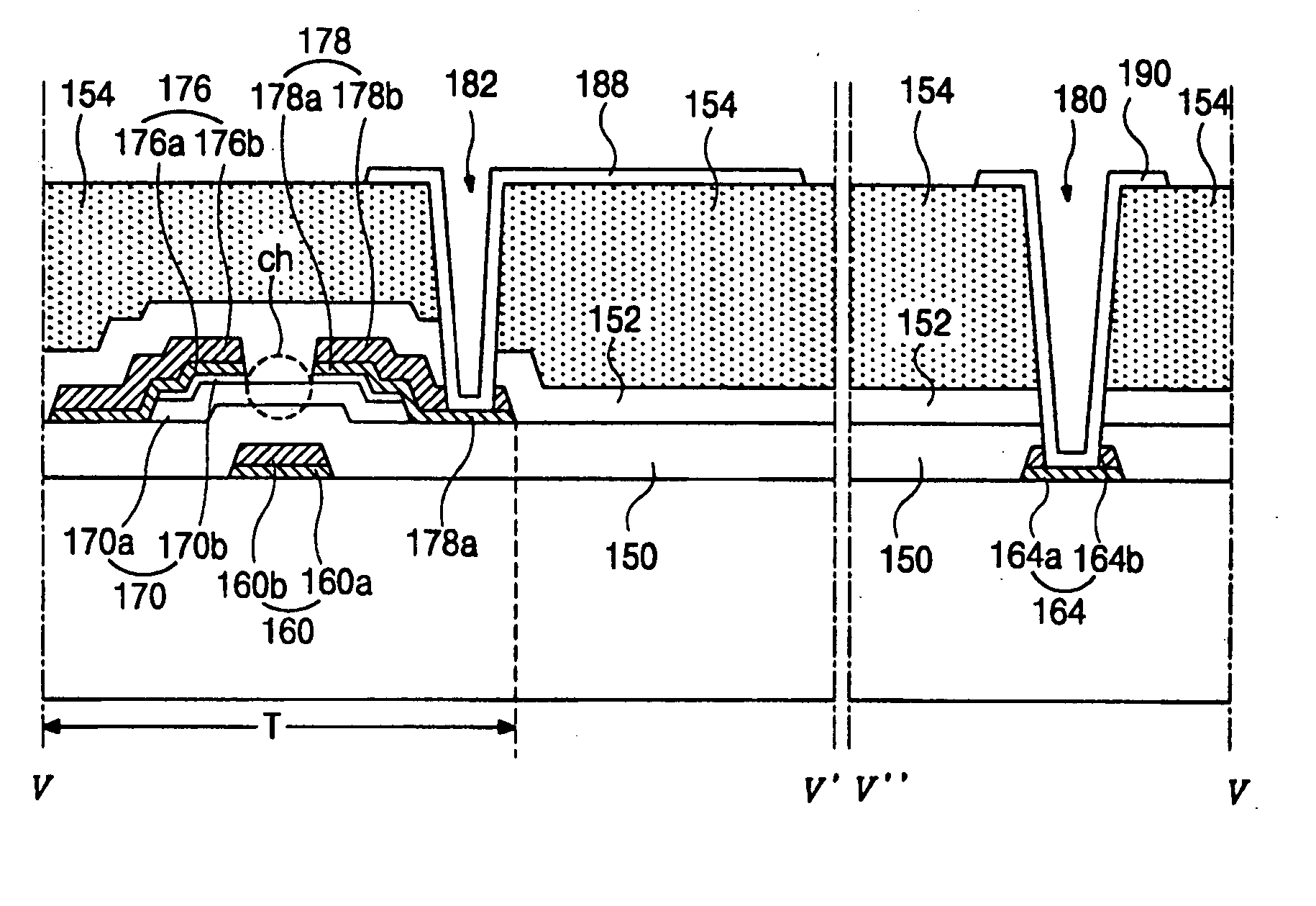
[0033]FIG. 4 is a schematic plan view of an array substrate for a liquid crystal display device according to an exemplary embodiment of the present invention.

[0034] In FIG. 4, a gate line 162 and a data line 174 crossing each other are formed on a substrate (not shown). A thin film transistor “T” including a gate electrode 160, an active layer 170, and source and drain electrodes 176 and 178 is formed at a crossing point of the gate and data lines 162 and 174. A gate pad 164 and a data pad 173 are formed at ends of the gate and data lines 162 and 174, respectively. The gate and data lines 162 and 174 have a double-layered structure of a copper layer as an upper layer and a barrier layer as a lower layer....


PUM

PropertyMeasurementUnit
dielectric constantaaaaaaaaaa
temperatureaaaaaaaaaa
insulatingaaaaaaaaaa

Abstract

An array substrate for a liquid crystal display device includes: a substrate; a gate electrode on the substrate; a gate insulating layer on the gate electrode; a semiconductor layer on the gate insulating layer; source and drain electrodes on the semiconductor layer, the source and drain electrodes including a copper layer as an upper layer and a barrier layer as a lower layer; a first passivation layer on the source and drain electrodes; a second passivation layer on the first passivation layer, the second passivation layer having a drain contact hole through the first passivation layer, the drain contact hole exposing the barrier layer; and a pixel electrode connected to the barrier layer through the drain contact hole.

Description

[0001] This application claims the benefit of Korean Patent Application No. 2001-86429, filed on Dec. 27, 2001, which is hereby incorporated by reference for all purposes as if fully set forth herein. BACKGROUND OF THE INVENTION [0002] 1. Field of the Invention [0003] The present invention relates to a liquid crystal display (LCD) device, and more particularly to an array substrate for an LCD device having an improved contact property. [0004] 2. Discussion of the Related Art [0005] LCD devices are developed as next generation display devices because of their lightweight, thin profile, and low power consumption characteristics. In general, an LCD device is a non-emissive display device that displays images using a refractive index difference having optical anisotropy properties of liquid crystal material that is interposed between a thin film transistor (TFT) array substrate and a color filter (C / F) substrate. Presently, among the various type of LCD devices commonly used, active mat...

Claims


Application Information

Patent Timeline
Patent Type & Authority Applications(United States)
IPC IPC(8): G02F1/1362H01L21/336G02F1/1333H01L21/77H01L21/84H01L27/12H01L29/45H01L29/49
CPCG02F1/13458G02F1/136227G02F2001/13629G02F2001/136295H01L27/124H01L29/458H01L29/4908H01L29/66765H01L27/12G02F1/13629G02F1/136295G02F1/1333
Inventor CHAE, GEE SUNG
Owner LG DISPLAY CO LTD
Features
  • Generate Ideas
  • Intellectual Property
  • Life Sciences
  • Materials
  • Tech Scout
  • Unparalleled Data Quality
  • Higher Quality Content
  • 60% Fewer Hallucinations
Learn More