

Fabrication process for a semiconductor device having a metal oxide dielectric material with a high dielectric constant, annealed with a buffered anneal process
a technology of metal oxide dielectric material and fabrication process, which is applied in the direction of coating, capacitor, chemical vapor deposition coating, etc., can solve the problems of shortened battery life of portable devices such as cellular telephones and laptop computers, leakage of charge carriers, and longer functions as effective insulators, so as to achieve the effect of driving current and high carrier mobility
- Summary
- Abstract
- Description
- Claims
- Application Information
AI Technical Summary
Benefits of technology
Problems solved by technology
Method used
Image

Examples
Embodiment Construction
[0023] The present invention will be understood from the following detailed discussion of exemplary embodiments which is presented in connection with the accompanying drawings.
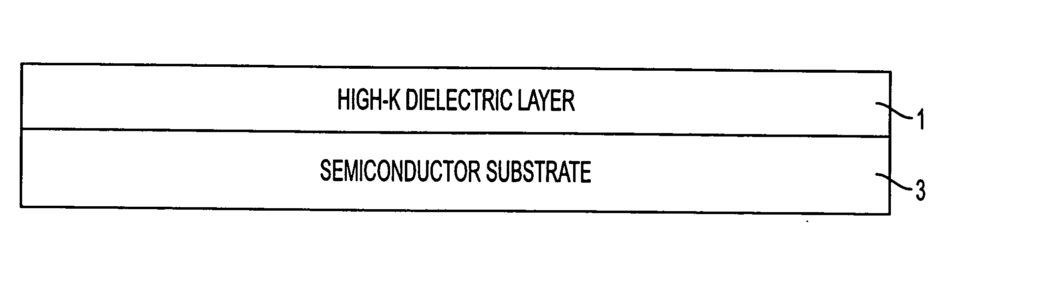
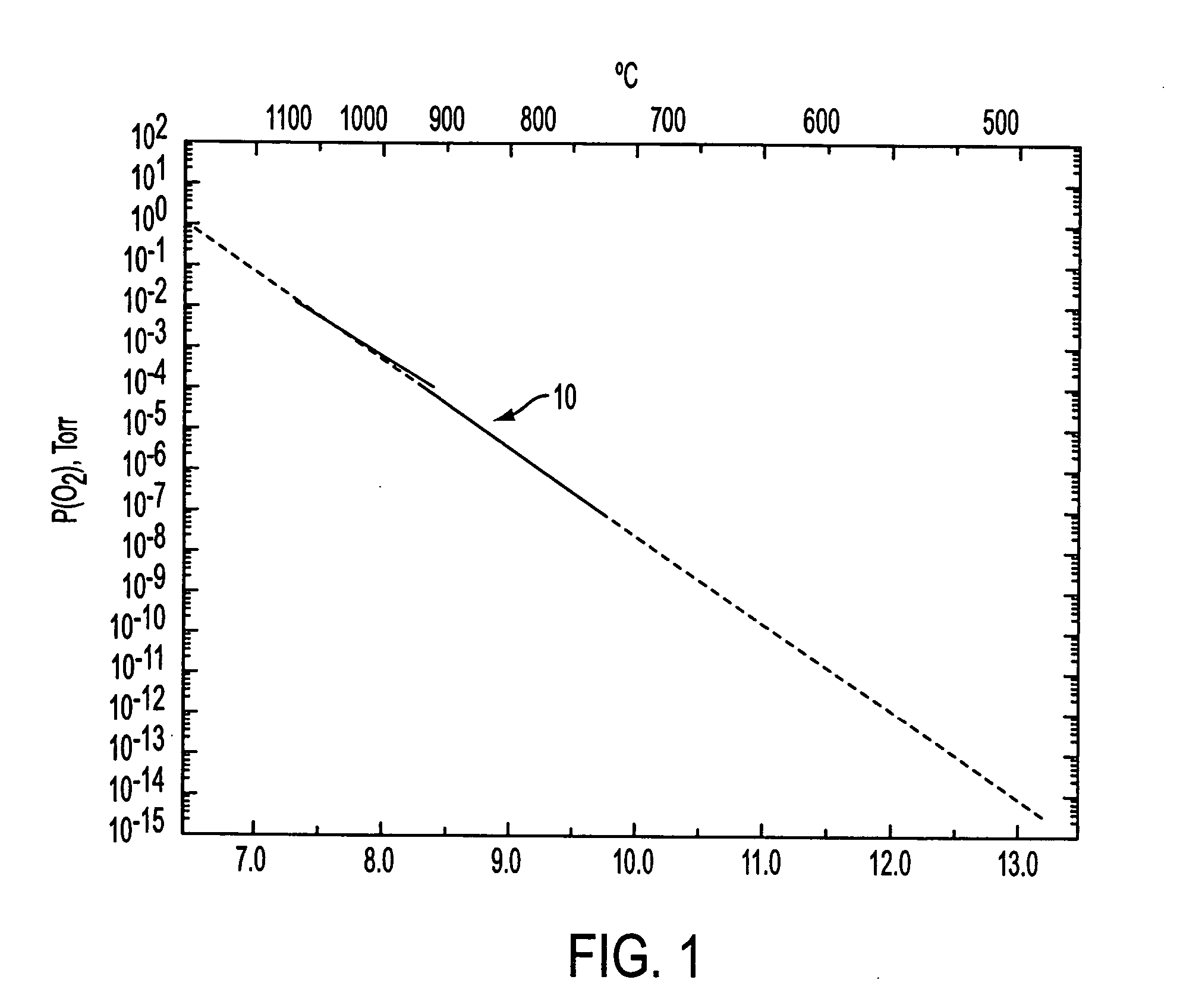
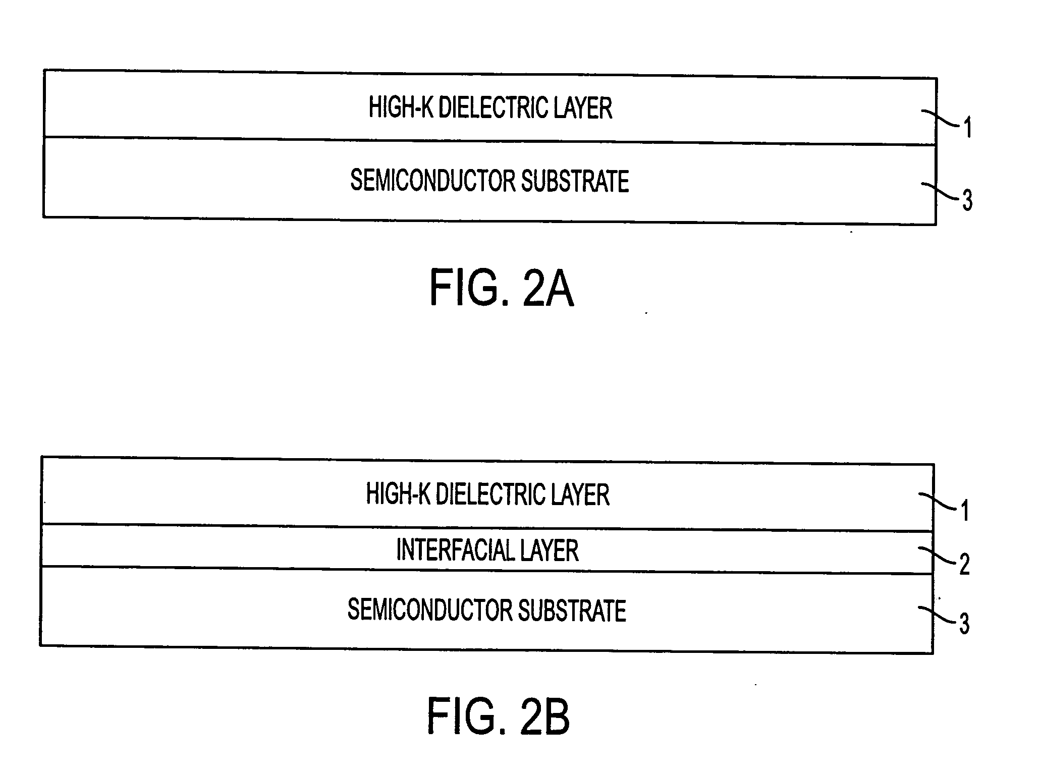
[0024] The present invention provides a method of fabricating a semiconductor device having a metal oxide dielectric layer with a high dielectric constant (high-K), annealed with a buffered anneal process. An interfacial layer such as SiO2 is optionally present between the metal oxide layer and substrate during the buffered anneal process. The buffered anneal process anneals the metal oxide dielectric layer in an oxygen atmosphere in which the partial pressure of oxygen is controlled as a function of anneal temperature such that annealing occurs under conditions at or below the thermodynamic chemical equilibrium for SiO / SiO2 and at or above the thermodynamic chemical equilibrium for the metal oxide dielectric layer.
[0025] In the following description, specific details such as layer thicknesses, material comp...
PUM
| Property | Measurement | Unit |
|---|---|---|
| Dielectric polarization enthalpy | aaaaa | aaaaa |
| Equilibrium | aaaaa | aaaaa |
| Electric charge | aaaaa | aaaaa |
Abstract
Description
Claims
Application Information