Plating method and plating solution

Inactive Publication Date: 2005-03-03
EBARA CORP +1
View PDF7 Cites 50 Cited by
  • Summary
  • Abstract
  • Description
  • Claims
  • Application Information

AI Technical Summary

Benefits of technology

[0007] The present inventors have noticed that in order to embed copper by plating in interconnect recesses (vias or interconnect trenches) having an aspect ratio of at least 1, it is necessary to moderate the concentration of electric current in the openings of the interconnect recesses. As

Problems solved by technology

As a consequence, the openings can be closed before the interconnect recesses is embedded with c

Method used


Image

  • Plating method and plating solution
  • Plating method and plating solution
  • Plating method and plating solution

Examples


example 1

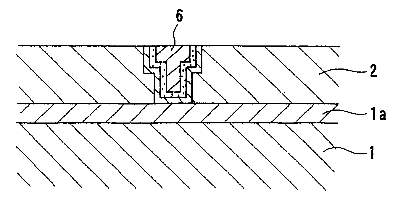
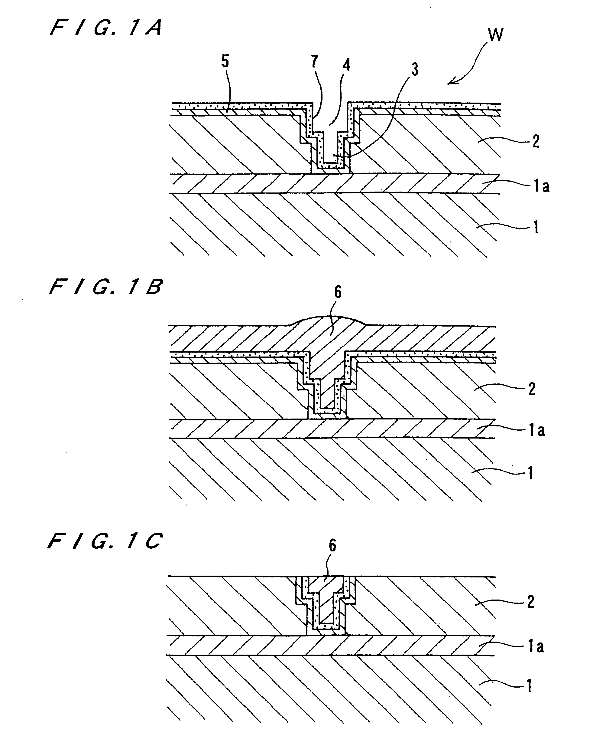
[0030] Using a copper sulfate plating solution having the composition described below, plating was carried out onto a surface of a silicon wafer having vias with a diameter of 40 μm and an aspect ratio of 1.5, and having a seed layer (conductive film) which has been formed in the usual manner. As a result, the vias were completely filled with copper. Further, observation of the interior of the via, after cutting the via, revealed no formation of void in the copper.

[0031]

CuSO4.5H2O200 g / LH2SO4 10 g / LCl 60 ppmPEG200 ppm

[0032] (Molecular Weight: about 3000)

SPS5 ppmPolyethyleneimine1 ppm

[0033] (Molecular Weight: about 10,000)

[0034]

Liquid temp.25° C.Current density10 mA / cm2Plating time 3 hrsStirringat 400 rpm (with a stirrer)

[0035] The plating method of the present invention makes it possible to embed copper in vias having an opening size of several tens of μm and an aspect ratio of at least 1.5 without the formation of voids.

[0036] Accordingly, the plating method can be advantageou...


PUM

PropertyMeasurementUnit
Concentrationaaaaaaaaaa
Widthaaaaaaaaaa
Dissociation constantaaaaaaaaaa

Abstract

The present invention provides a plating method which can embed copper in interconnect recesses, such as vias and interconnect trenches, having an opening width or size of several tens of μm and an aspect ratio of at least 1.5. The plating method comprises: providing a substrate having interconnect recesses, whose surfaces are covered with a conductive layer, formed in a surface of the substrate; bringing the surface of the substrate into contact with a plating solution containing copper ions, an organic or inorganic acid, chloride ions, a polymeric surfactant for suppressing electrodeposition, a sulfur-containing saturated organic compound for promoting the growth of a plated film, and a nitrogen-containing polymer for flattening a surface of the plated film; and applying a voltage between the conductive layer and an anode immersed in the plating solution.

Description

BACKGROUND OF THE INVENTION [0001] 1. Field of the Invention [0002] The present invention relates to a plating method for embedding copper (Cu) in interconnect recesses (circuit pattern) formed in a surface of a substrate, such as a semiconductor substrate, a printed circuit board, or a CSP (chip-size-package) substrate, or the like, and to a plating solution for use in the plating method. The plating method of the present invention is useful especially for embedding copper in interconnect recesses, having an opening width or size of not less than 1 μm and an aspect ratio of at least 1, without the formation of voids. [0003] 2. Description of the Related Art [0004] Interconnect recesses, such as interconnect trenches and vias, having an opening width or size of several tens of μm and an aspect ratio of at least 1.5, are employed in the actual formation of interconnects, and the aspect ratio is expected to become larger in the future. There is now a demand for embedding copper, by pl...

Claims


Application Information

Patent Timeline
IPC IPC(8): C25D3/38C25D5/02C25D7/12H01L21/288H01L21/445H01L21/768H05K3/18H05K3/42
CPCC25D3/38H05K3/423H01L21/76877H01L21/2885
Inventor SAHODA, TSUYOSHINAKADA, TSUTOMUMISHIMA, KOJIKIMIZUKA, RYOICHI
Owner EBARA CORP
Why Eureka
Try Eureka