

Optical scanning device and image forming apparatus using the same
a scanning device and image forming technology, applied in the direction of inking apparatus, instruments, electrographic processes, etc., can solve the problems of increasing cost, difficult to make the wavelengths completely equal to one another, and limitation of the selection range of wavelengths of light sources, so as to achieve convenient production and improve performance
- Summary
- Abstract
- Description
- Claims
- Application Information
AI Technical Summary
Benefits of technology
Problems solved by technology
Method used
Image

Examples
first embodiment
(First Embodiment)
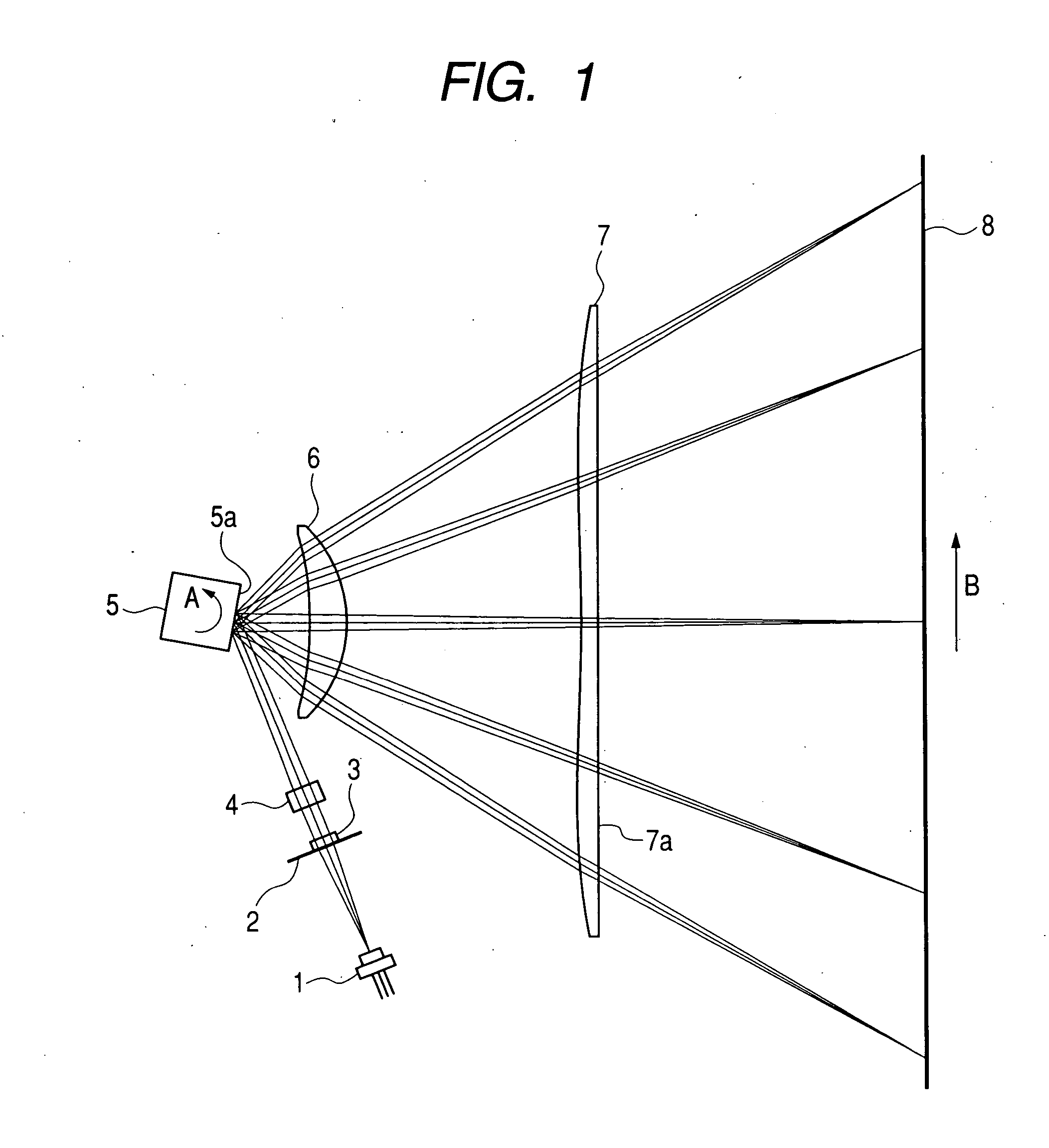
FIG. 1 is a main scanning sectional view showing an optical scanning device according to a first embodiment of the present invention.
Here, a main scanning direction indicates a direction perpendicular to the rotational axis of deflecting means. A sub scanning direction indicates a direction parallel to the rotational axis of the deflecting means. In addition, a main scanning section indicates a plane which is parallel to the main scanning direction and includes the optical axes of a deflection optical element (lens) 6 and a diffraction optical element (lens) 7 having a diffraction grid 7a formed on an exit surface of a diffraction part, which compose a scanning optical system.
A divergent light flux emitted from a single beam semiconductor laser 1 serving as light source means is limited by a diaphragm 2 so as to reduce a width of the light flux, thereby obtaining a desirable spot size. Then, the light flux is converted into a substantially parallel light flux b...
second embodiment
(Second Embodiment)
FIG. 8 is an explanatory view showing an optical scanning device according to a second embodiment of the present invention, which shows an embodiment in which a diffraction grid is formed in the cylinder lens 4. In this embodiment, a diffraction grid 4a is formed on an exit surface side of the cylinder lens 4 and has power in only the sub scanning direction. The cylinder lens 4 itself is made of an optical resin and can be produced at low cost by injection molding.
Table 4 shows curvatures of the cylinder lens 4, phase coefficients of the diffraction grid 4a, and the like.
The phase function used here is the same as in the first embodiment.
φ=2πk / λ·d0·Z2 (k=2 and λ=405 nm)
In this embodiment, the diffraction grid 4a is constructed using the second design order as in the first embodiment.
With respect to the diffraction grid used here, m·L·λ=111 and P / λ=56.35. Therefore, both Expression 1 and Expression 2 are satisfied. When the present invention is applied to ...
third embodiment
(Third Embodiment)
FIG. 9 is an explanatory view showing a part of an optical scanning device according to a third embodiment of the present invention, which shows an embodiment in which a diffraction grid is formed in the collimator lens 3. In this embodiment, a diffraction grid 3a is formed on an incident surface side of the collimator lens 3. Because of a concentric diffraction grid, although the single collimator lens is used, it becomes an optical system in which an on-axis chromatic aberration is corrected.
Table 5 shows curvatures of the collimator lens 3, phase coefficients of the diffraction grid 3a, and the like.
The phase function used here is the same as in the first embodiment.
φ=2πk / λ·c0·H2, H2=Y2+Z2 (k=2 and λ=405 nm)
In this embodiment, the diffraction grid 3a is constructed using the second design order as in the first and second embodiments.
With respect to the diffraction grid 3a used here, m·L·λ=47 and P / λ=129.60. Therefore, both Expression 1 and Expression 2 ...
PUM
 Abstract
Description
Claims
Application Information