Testing apparatus using charged particles and device manufacturing method using the testing apparatus

a technology of testing apparatus and charged particles, applied in the field of testing apparatus, can solve the problems of poor conduction, inferior throughput of the inspection apparatus of the electron beam type, and disadvantages of the inspection apparatus of the optical typ

Active Publication Date: 2005-03-03
EBARA CORP
View PDF6 Cites 401 Cited by
  • Summary
  • Abstract
  • Description
  • Claims
  • Application Information

AI Technical Summary

Problems solved by technology

Furthermore, as the device is increasingly multilayered, the inspection apparatus is required to have a function of detecting a contact failure (electric defects) of vias for connection of wiring between layers.
However, the electron beam-type defect inspection apparatus has a disadvantage, i.e. it is inferior in throughput to the optical type.
The electron beam type has a remarkable characteristic such that electric defects (breakage of wiring, poor conduction, poor conduction of vias and the like) can be inspected, but the inspection speed is very low, and development of a defect inspection apparatus performing inspection at a high speed is expected.
Generally, the inspection apparatus is expensive, inferior in throughput to other process apparatuses, and is therefore used after an important step, for example, etching, film formation, or CMP (chemical mechanical polishing) planarization processing under present circumstances.
The serious problem is that this inspection speed is very low compared to the optical type ({fraction (1 / 20)} or less of that of the optical type).

Method used


Image

  • Testing apparatus using charged particles and device manufacturing method using the testing apparatus
  • Testing apparatus using charged particles and device manufacturing method using the testing apparatus
  • Testing apparatus using charged particles and device manufacturing method using the testing apparatus

Examples


embodiment 1

(1) Embodiment 1

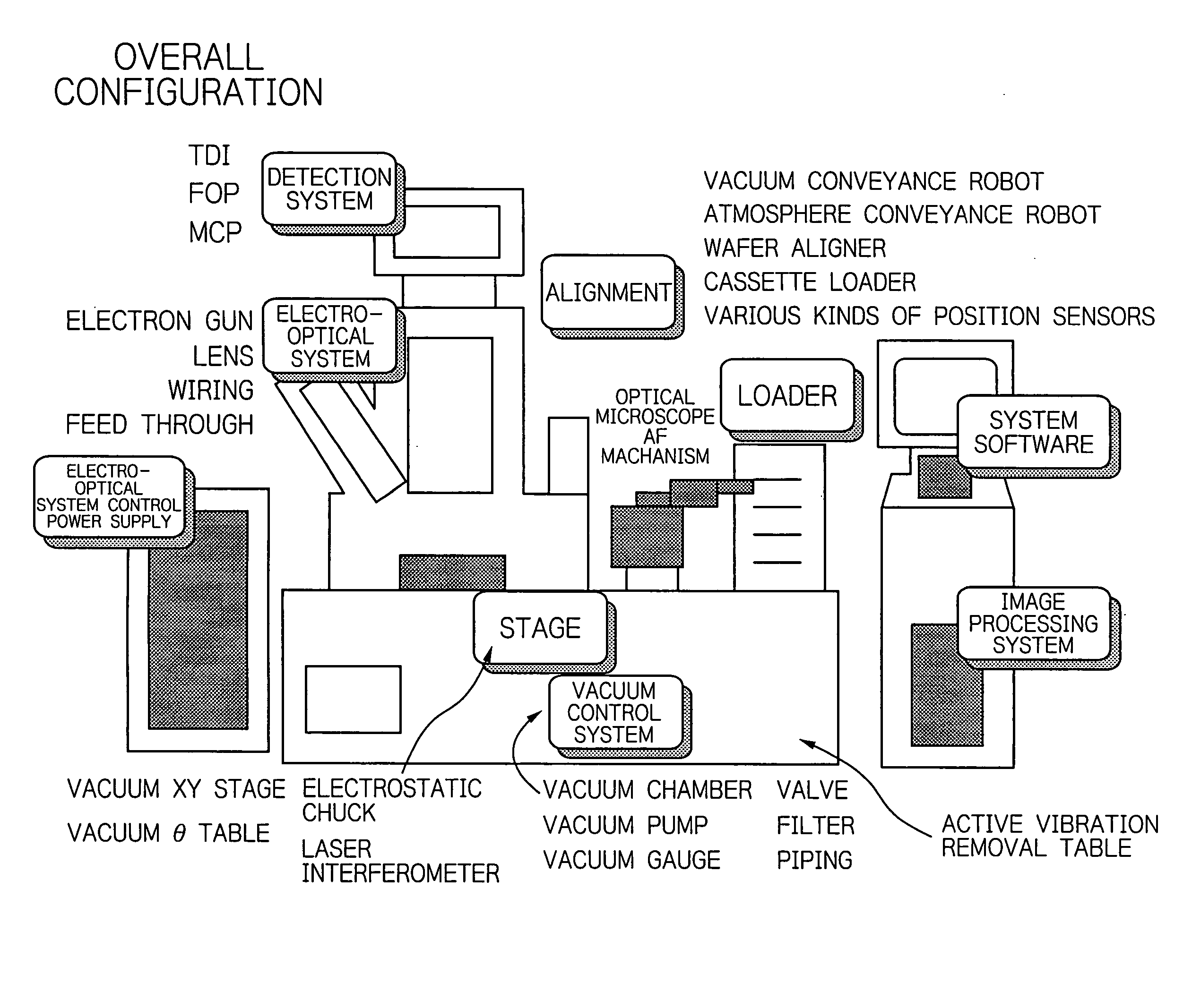
The embodiment is one example of inspection apparatus mainly comprised of a vacuum chamber, a vacuum pumping system, a primary optical system, a secondary optical system, a detector, an image processing unit and a computer for control. One example thereof is shown in FIG. 26.

A primary optical system 26•1 for illuminating an electron beam to a sample, and a secondary optical system 26•2 for guiding electrons emitted from the sample surface, for example secondary electrons, reflection electrons, back-scattered electrons, to the detector are provided. The secondary optical system is a projection electron microscope type optical system. A beam separator 26•3 of E×B is used for separating the primary system and the secondary system. Furthermore, an image signal of an electron detected by a detector 26•4 is an optical signal or / and an electric signal, and processed by an image processing unit 26•5. Furthermore, at this time, if the number of electrons entering the detec...

embodiment 2

(2) Embodiment 2

When the TDI sensor / camera is used for the detector in the inspection apparatus similar to the embodiment 1, the image can be acquired more quickly and efficiently if the number of images / stages is 2048 to 4096, the number of taps is 32 to 128, and the sensitivity is 10000 to 40000 DN / (nJ / cm2). At this time, the line rate may be 100 to 400 kHz, and the video rate may be 10 MHz to 40 MHz. At this time, the operation is capable of being done when an 8 inch Si wafer, for example LSI device wafer is used, the resolution is 0.1 μm / pixel, and inspection time per one wafer is ⅛ to 2 hours.

At this time, when the resolution is 0.1 μm / pixel, a contrast of 3 to 30% is achieved, and thus image observation and defect detection can be sufficiently performed even with a pattern shape of, for example, LS:0.2 / 0.2 μm in sample observation and defect inspection. A defect having a shape other than L / S can be detected by comparison using a change in contrast as long as the defect has ...

embodiment 3

(3) Embodiment 3

In this embodiment, an EB-CCD or EB-TDI is used for the detector (see FIG. 30) in the embodiments 1 and 2. The EB is an electron beam, and the EB-CCD or EB-TDI directly inputs the electron beam, and converts it into an electric signal (not detecting an optical signal).

Use of the EB-TDI sensor / camera can inject electrons directly into an image portion of the sensor, accumulate charges. This means that it is unnecessary to use the fluorescent screen, the relay lens and hermetic glass used in the usual detector. That is, since an electric signal can be obtained directly from an electron signal without temporarily converting an electron signal image into an optical signal image, and thus a loss associated with the conversion can be considerably reduced. That is, image deformation by the fluorescent screen, hermetic glass and the relay lens system, degradation in contrast, and deleterious effects such as variations in magnification can be considerably reduced. Furtherm...


PUM

PropertyMeasurementUnit
current densityaaaaaaaaaa
energyaaaaaaaaaa
line frequencyaaaaaaaaaa

Abstract

A system for further enhancing speed, i.e. improving throughput in a SEM-type inspection apparatus is provided. An inspection apparatus for inspecting a surface of a substrate produces a crossover from electrons emitted from an electron beam source 25••1, then forms an image under a desired magnification in the direction of a sample W to produce a crossover. When the crossover is passed, electrons as noises are removed from the crossover with an aperture, an adjustment is made so that the crossover becomes a parallel electron beam to irradiate the substrate in a desired sectional form. The electron beam is produced such that the unevenness of illuminance is 10% or less. Electrons emitted from the sample W are detected by a detector 25•11.

Description

BACKGROUND OF THE INVENTION 1. Field of the Invention The present invention relates to an inspection apparatus inspecting defects or the like of a pattern formed on the surface of an inspection object using an electron beam, and particularly relates to an inspection apparatus irradiating an electron beam to the inspection object and capturing secondary electrons modified according to properties of the surface thereof to form image data, and inspecting in high throughput a pattern or the like formed on the surface of the inspection object based on the image data, and a device production process of producing a device in a high yield using the inspection apparatus as used for detection of wafer defects in semiconductor manufacturing. More specifically, the present invention relates to a detection apparatus with a projection electron microscope system using broad beams, and a device production process using the apparatus. In a semiconductor process, the design rule is about to move i...

Claims


Application Information

Patent Timeline
Patent Type & Authority Applications(United States)
IPC IPC(8): G01N23/225H01J37/05H01J37/28
CPCG01N23/225H01J37/05H01J37/28H01L2223/54466H01J2237/2446H01J2237/2817H01L21/6833H01J2237/2441G01N23/2204H01J37/20H01J2237/202H01J2237/2801
Inventor NOJI, NOBUHARUSATAKE, TOHRUSOBUKAWA, HIROSIKIMBA, TOSHIFUMIHATAKEYAMA, MASAHIROYOSHIKAWA, SHOJIMURAKAMI, TAKESHIWATANABE, KENJIKARIMATA, TSUTOMUSUEMATSU, KENICHITABE, YUTAKATAJIMA, RYOTOHYAMA, KEIICHI
Owner EBARA CORP
Why Eureka
Try Eureka