Semiconductor device

a technology of semiconductor devices and semiconductors, applied in the field of semiconductor devices, can solve the problems of increasing the probability of design failure, increasing the cost of masks, and re-designing interconnection patterns or mask formulations, so as to reduce the cost, reduce the chip area, and high the effect of logic circuit utilization efficiency

Inactive Publication Date: 2005-03-03
NEC CORP
View PDF6 Cites 272 Cited by
  • Summary
  • Abstract
  • Description
  • Claims
  • Application Information

AI Technical Summary

Benefits of technology

[0008] In a programmable semiconductor integrated circuit, such as FPGA, the circuit structure can be changed by changing the memory storage contents. However, the circuit suffers from a problem that the memory devices occupy an extremely large area. The result is that the programmable semiconductor integrated circuit has an increased chip area, such that it is extremely expensive. Moreover, the FPGA, in which the memory devices take-up a large area, the interconnection switches, used for changing the connection of logic circuits or arithmetic circuits, take-up a large area, thereby lowering the proportion of the area of the logic circuit or the arithmetic circuit in the entire chip surface. Thus, in the routine FPGA, as many functions as possible are allotted to one logic circuit or one arithmetic circuit to raise the granularity of the logic or arithmetic circuit and hence the proportion of the logic or arithmetic circuit in the entire chip area. However, the logic circuit or arithmetic circuit with a coarse granularity tends to produce wastefulness, depending on the allocated functions, thus lowering the utilization efficiency.
[0026] With the switch element of the present invention, in distinction from the switch element formed on a substrate, the power consumption may be diminished, because there is no leak current flowing in the substrate.

Problems solved by technology

If, in a conventional semiconductor integrated circuit, a design failure has been found, or a design has been changed, after fabrication, the circuit must be re-fabricated after re-designing the interconnection pattern.
In case of a design change, tremendous costs are incurred in re-designing the interconnection pattern or in mask formulation.
In keeping with the increase in the scale of the integrated circuit, the probability of occurrence of design failure is increasing, while the cost of the mask is increasing rapidly with the progress of process minituarization.
However, the circuit suffers from a problem that the memory devices occupy an extremely large area.
The result is that the programmable semiconductor integrated circuit has an increased chip area, such that it is extremely expensive.
However, the logic circuit or arithmetic circuit with a coarse granularity tends to produce wastefulness, depending on the allocated functions, thus lowering the utilization efficiency.
Among the problems that may be presented in near future, there is a problem of the increase in power consumption due to leak current from the memory device, and destruction of storage contents by cosmic-ray-induced soft error.

Method used


Image

  • Semiconductor device
  • Semiconductor device
  • Semiconductor device

Examples


embodiments

[0113] The embodiments of the present invention, in which the switch element according to the present invention, explained in the above preferred embodiment, has been applied to a programmable logic circuit and to a memory circuit, are now explained with reference to the drawings.

[0114]FIG. 5 shows the structure of an embodiment of a programmable logic circuit of the present invention, employing a switch element of the present invention.

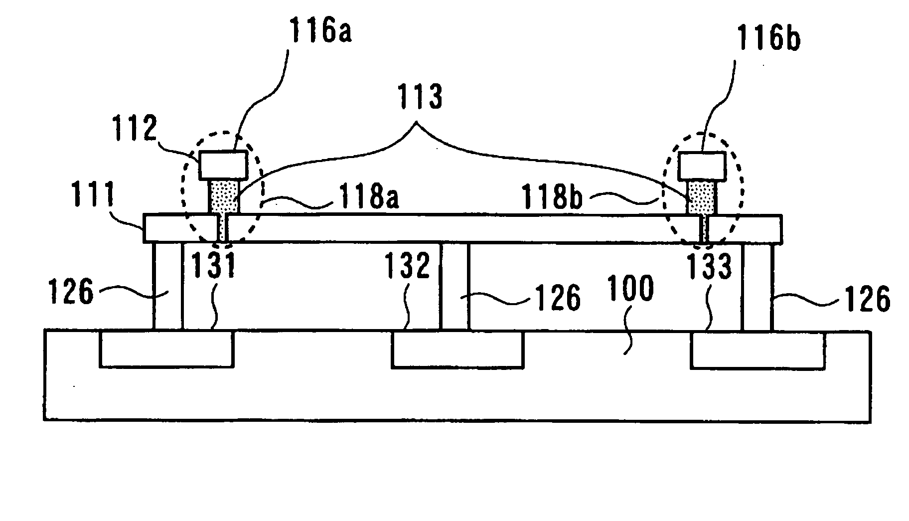
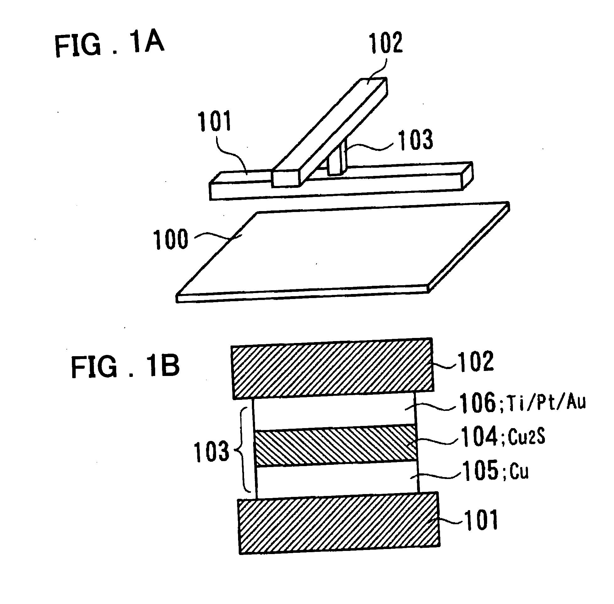
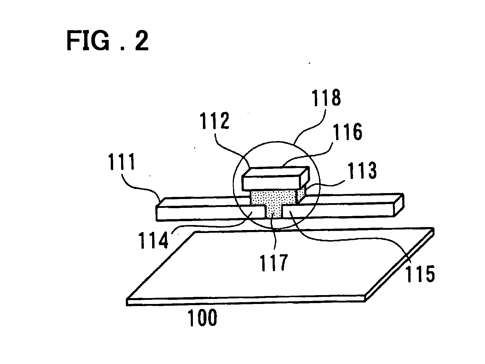
[0115] Referring to FIG. 5, a semiconductor integrated circuit of the present embodiment includes a plural number of input terminals 150, a selector circuit 151, a plural number of switch elements 152, a sense circuit 152, a sense circuit 153, and an output terminal 154. The switch elements 152 are each formed by the via 103, shown in FIGS. 1 and 3, or by the switch element 118, shown in FIGS. 2 and 4, formed in an interconnection layer, and the electrical conductivity across two terminals thereof may be changed.

[0116] The selector circuit 151 com...


PUM


Abstract

A programmable semiconductor device has a switch element in an interconnection layer, wherein in at least one of the inside of a via, interconnecting a wire of a first interconnection layer and a wire of a second interconnection layer, a contact part of the via with the wire of the first interconnection layer and a contact part of the via with the wire of the second interconnection layer, there is provided a variable electrical conductivity member, such as a member of an electrolyte material. The via is used as a variable electrical conductivity type switch element or as a variable resistance device having a contact part with the wire of the first interconnection layer as a first terminal and having a contact part with the wire of the second interconnection layer as a second terminal. By varying the electrical conductivity of the switch element, the state of connection of the via with the wire of the first interconnection layer and the state of connection of the via with the wire of the second interconnection layer may be variably set to a shorted state, an open-circuited state or to an intermediate state A two-state switch element includes an ion conductor for conducting metal ions interposed between the first and second electrodes. The second electrode is formed of a material lower in reactivity than the first electrode. The electrical conductivity across the first and second electrodes is changed by the oxidation-reduction reaction of the metal ions. There are provided first and second transistors of opposite polarities, connected to the first electrode, and third and fourth transistors of opposite polarities, connected to the second electrode.

Description

FIELD OF THE INVENTION [0001] This invention relates to a semiconductor device. More particularly, it relates to an interconnection structure of a programmable semiconductor device, a logic integrated circuit, an arithmetic circuit device and a memory device having such interconnection structure, and a programming circuit therefor. BACKGROUND OF THE INVENTION [0002] A conventional semiconductor integrated circuit is composed of transistors formed on a semiconductor substrate, and an interconnection structure, formed as an upper layer of the semiconductor substrate for interconnecting the elements. The interconnection pattern is determined at the designing stage of the integrated circuit, and hence the connecting states of the transistors cannot be changed after the fabrication of the semiconductor integrated circuit. [0003] The above problem can be solved with a programmable semiconductor integrated circuit, such as FPGA (field programmable gate array). With the programmable semicon...

Claims


Application Information

Patent Timeline
Patent Type & Authority Applications(United States)
IPC IPC(8): G11C11/56G11C13/00G11C11/412G11C13/02H01L23/525H01L27/10H01L27/105H01L27/11H01L27/24H01L29/06H01L29/66H01L45/00H03K19/177
CPCG11C11/5614G11C13/0011H01L2924/0002G11C13/003G11C13/004G11C2013/0054G11C2213/71G11C2213/72G11C2213/75G11C2213/76G11C2213/77G11C2213/79H01L23/5252H01L23/5256H01L27/11H01L27/24H01L2924/3011H03K19/17736H03K19/17748H03K19/1778H01L2924/00G11C2013/0066H10B63/20H10B63/30H10B63/80H10B63/84H10N70/253H10N70/245H10N70/826H10N70/8822H10B10/00H10B63/00
Inventor KAERIYAMA, SHUNICHIMIZUNO, MASAYUKI
Owner NEC CORP
Why Eureka
Try Eureka