Semiconductor device and fabricating method thereof

Inactive Publication Date: 2005-03-03
DONGBU ELECTRONICS CO LTD +1
View PDF8 Cites 20 Cited by
  • Summary
  • Abstract
  • Description
  • Claims
  • Application Information

AI Technical Summary

Benefits of technology

[0017] The object of the present invention is to provide a reliable semiconductor device and a fabricating method thereof w

Problems solved by technology

However, applying a constant voltage to the sidewall gates has several problems, in that: (1) a contact should be formed on the sidewall gates; (2) the implanted ions for controlling the threshold voltage of the sidewall gates may be diffused by a later thermal treatment and affect the threshold voltage of the main gate electrode; (3) parasitic capacitance may be generated between the sidewall gates and the main gate electrode, between the sidewall gates and a body, a

Method used


Image

  • Semiconductor device and fabricating method thereof
  • Semiconductor device and fabricating method thereof
  • Semiconductor device and fabricating method thereof

Examples


Embodiment Construction

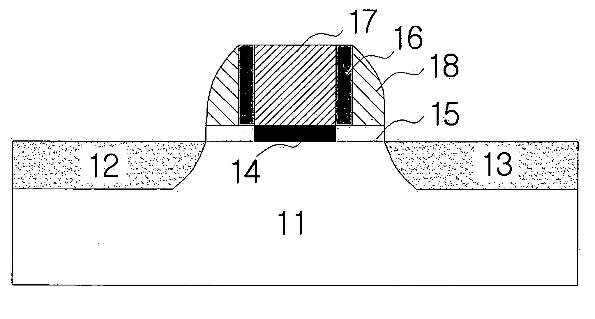
[0025] Reference will now be made in detail to the preferred embodiments of the present invention, examples of which are illustrated in the accompanying drawings.

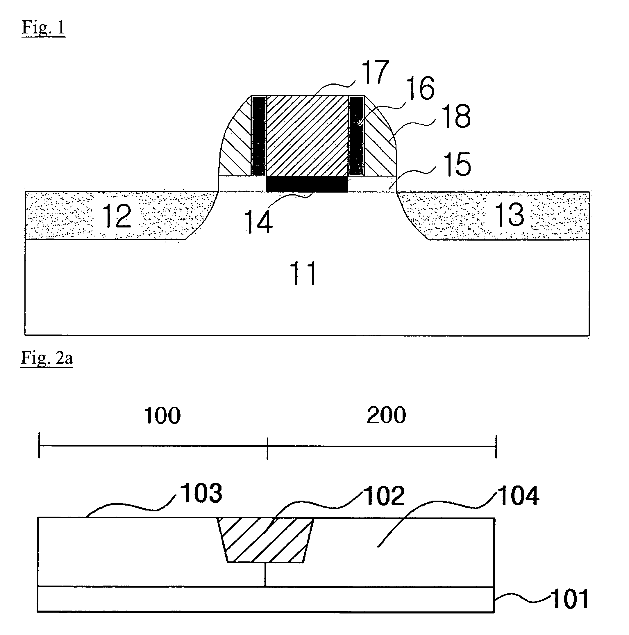
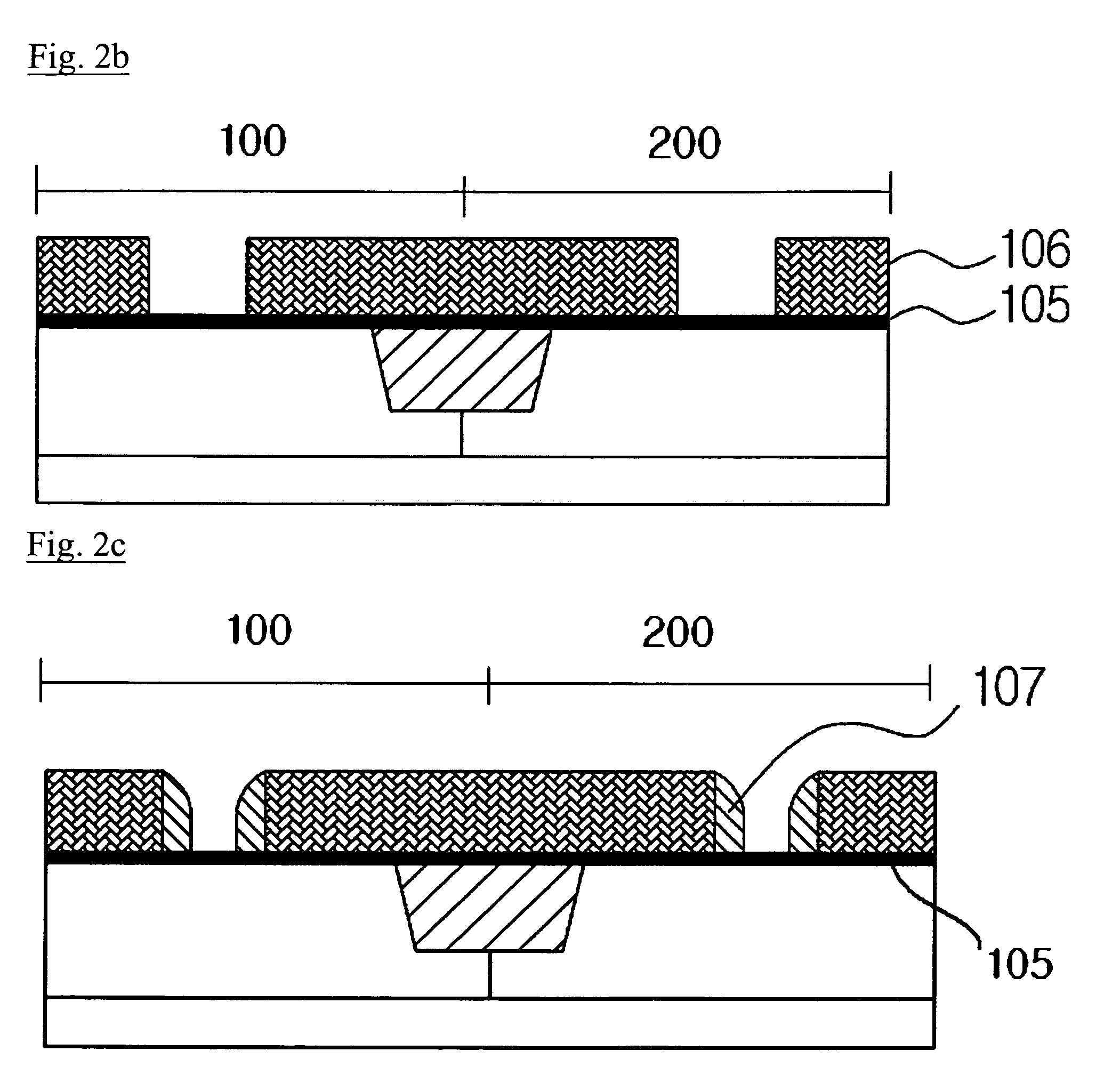
[0026]FIGS. 2a through 2k are cross-sectional views illustrating an example method for fabricating MOS transistors with virtual source / drain extension areas in accordance with the present invention.

[0027]FIG. 2a is a cross-sectional view illustrating a well formation process. A device isolation structure 102 is formed in a P-type substrate 101. The device isolation structure 102 electrically separates devices on the substrate. A photoresist layer is formed on the resulting structure, and a mask pattern is then formed by a photolithography process. With the mask pattern, a P-type well 103 is formed by implanting P-type impurity ions into a predetermined NMOS area 100. The mask pattern is then removed. With a photolithography process substantially identical to that for forming the P-type well 103 described above, an N-type ...


PUM


Abstract

A semiconductor device and a fabricating method thereof are disclosed. The semiconductor device includes polysilicon gate electrodes, a gate oxide layer, sidewall floating gates, a block oxide layer, source/drain areas, and sidewall spacers. In addition, the method includes the steps of: forming a block dielectric layer and a sacrificial layer on a semiconductor substrate; forming trenches by etching the sacrificial layer; forming sidewall floating gates on lateral faces of the trenches; forming a block oxide layer on the sidewall floating gates; forming polysilicon gate electrodes by a patterning process; removing the sacrificial layer; forming source/drain areas by implanting impurity ions into the resulting structure; injecting carriers or electric charges into the sidewall floating gates; and forming spacers on lateral faces of the polysilicon gate electrodes and the sidewall floating gates.

Description

BACKGROUND OF THE INVENTION [0001] 1. Field of the Invention [0002] The present disclosure relates to a semiconductor device and a fabricating method thereof and, more particularly, to nano-scale MOS transistors with virtual source / drain extension areas and a fabricating method thereof. [0003] 2. Background of the Related Art [0004] A conventional ion implantation method for forming a source / drain area has several shortcomings. One of these shortcomings is that implanted impurity ions can be diffused into a channel area by a later thermal treatment. Due to such a shortcoming, if the length of a gate electrode is equal to or less than 0.06 μm, a source area and a drain area may be easily connected through impurities, therefore preventing the fabrication of a MOS transistor. Even if the length of the gate electrode is more than 0.06 μm, a short channel effect may seriously occur because the shallow depth of the source / drain area is hardly formed to be less than 10 nm. Thus, to make a ...

Claims


Application Information

Patent Timeline
IPC IPC(8): H01L21/265H01L21/336H01L21/8238H01L21/8247H01L27/115H01L29/78
CPCH01L21/26586H01L21/823814H01L21/823828H01L21/823864H01L27/115H01L29/7833H01L29/66484H01L29/66553H01L29/66583H01L29/66643H01L29/7831H01L27/11521H10B69/00H10B41/30H01L21/18
Inventor JUNG, JIN HYO
Owner DONGBU ELECTRONICS CO LTD
Why Eureka
Try Eureka