Semiconductor storage device and refresh control method thereof
- Summary
- Abstract
- Description
- Claims
- Application Information
AI Technical Summary
Benefits of technology
Problems solved by technology
Method used
Image

Examples
Embodiment Construction
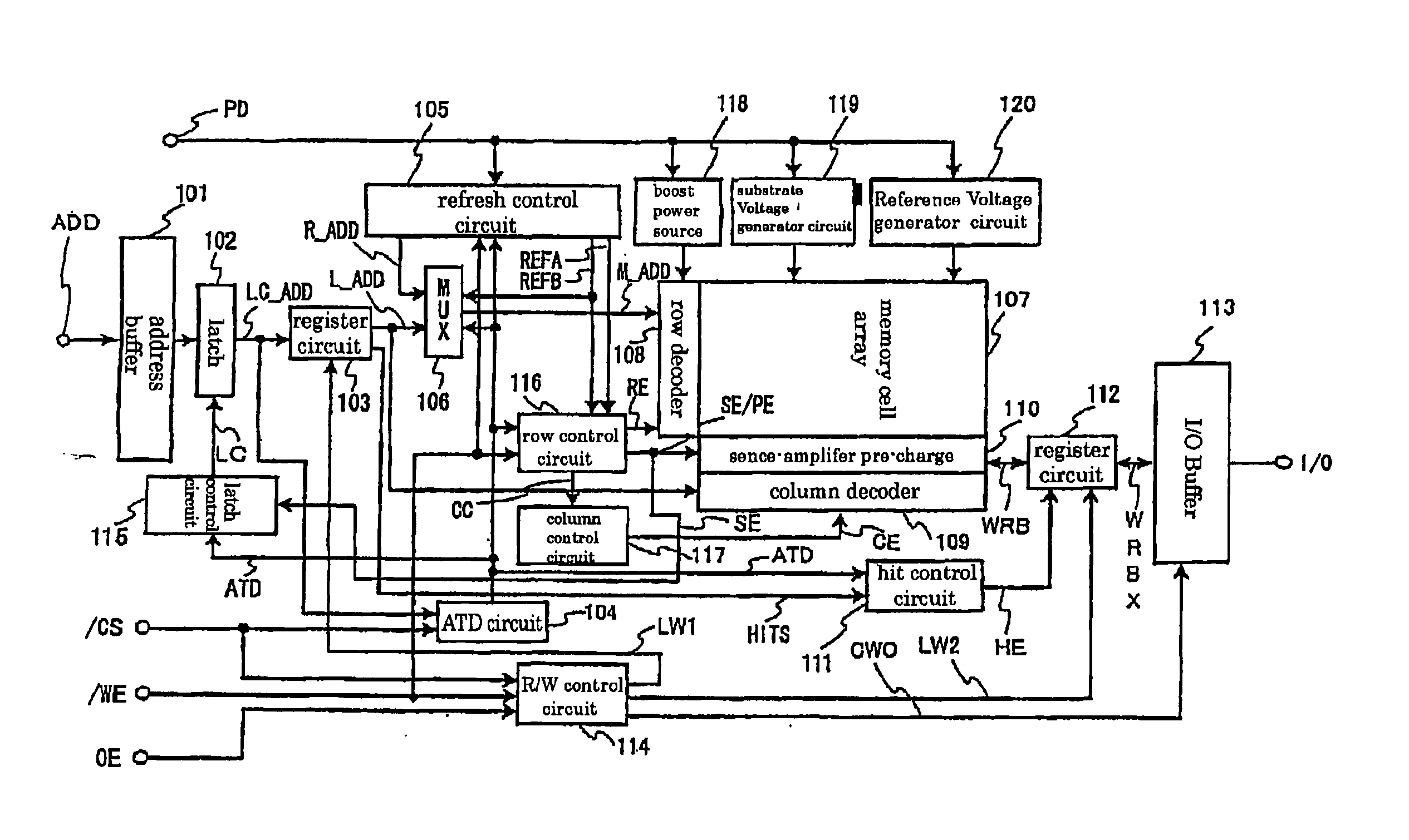
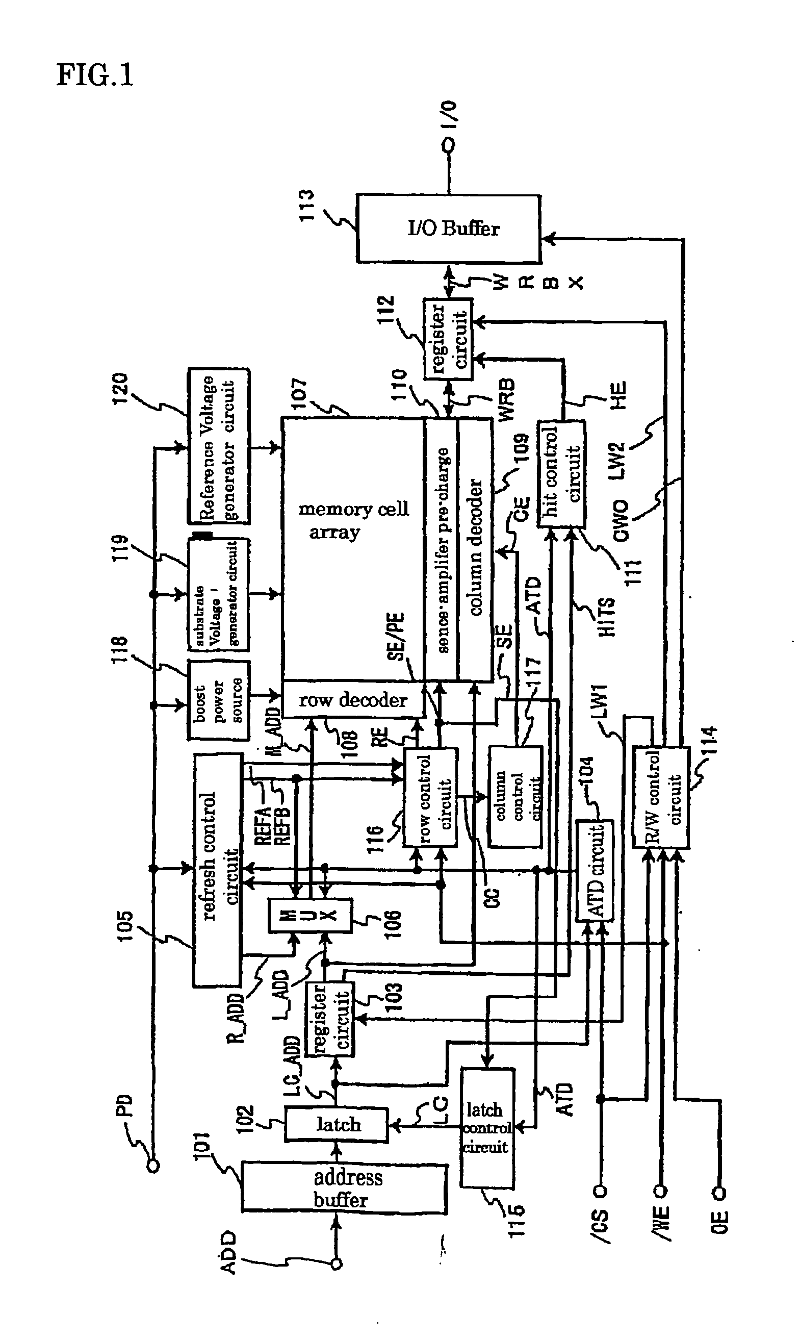
[0095]FIG. 3 is a diagram showing a configuration of a semiconductor memory device according to the first embodiment of the present invention.
[0096] In this figure, an address ADD is an access address supplied from outside of the semiconductor memory device. In accordance with an arrangement of a memory cell array 27 in a matrix form, the address ADD includes a row address (hereinafter referred to as X address) and a column address (hereinafter referred to as Y address). Address buffers 11 and 12 buffer the X address and Y address and output the same. Late write registers 13 and 14 has a register for late write and a latch circuit 102 in FIG. 1. The late write registers 13 and 14 include therein registers (address register) for holding access addresses equal in bit width to the X address and the Y address, respectively.
[0097] An address outputted from the late write register 14 for Y address is inputted to a Y predecoder 36 as an address Y-ADD for memory access, decoded into a plu...
PUM
 Abstract
Description
Claims
Application Information
 - Generate Ideas
- Intellectual Property
- Life Sciences
- Materials
- Tech Scout
- Unparalleled Data Quality
- Higher Quality Content
- 60% Fewer Hallucinations
Browse by: Latest US Patents, China's latest patents, Technical Efficacy Thesaurus, Application Domain, Technology Topic, Popular Technical Reports.
© 2025 PatSnap. All rights reserved.Legal|Privacy policy|Modern Slavery Act Transparency Statement|Sitemap|About US| Contact US: help@patsnap.com