Use of deep-level transitions in semiconductor devices

a technology of semiconductor devices and transitions, applied in semiconductor lasers, solid-state devices, semiconductor lasers, etc., can solve the problems of insufficient integration of inp circuits, high cost, and inability to achieve a level of device integration, so as to enhance carrier transport, enhance carrier transport, and enhance carrier transport

Inactive Publication Date: 2005-03-17
YALE UNIV
View PDF1 Cites 17 Cited by
  • Summary
  • Abstract
  • Description
  • Claims
  • Application Information

AI Technical Summary

Benefits of technology

In general terms, the invention relates to the design, fabrication, and use of semiconductor devices that employ deep-level transitions (i.e., deep-level-to-conduction-band, deep-level-to-valence-band, or deep-level-to-deep-level) to achieve useful results. To facilitate the “engineering” of useful devices based on deep-level transitions, it is important to (i) dispel the traditional (and pervasive) misunderstandings about deep-center transitions and (ii) provide a reliable analytical model to predict the device-relevant properties of such transitions.
In accordance with one aspect of the invention, design of useful deep-level devices is facilitated by a novel, eight-band {overscore (k)}∘{overscore (p)} model of deep-center states. This model exhibits good agreement with experimental measurements, and allows device designers to predict both the size and spectral shape of the strength of deep-level optical transitions to (i) the conduction band and / or (ii) the valence band, as well as (iii) optical-selection-rules, (iv) and the spatial extent of the deep-level bound state, (v) for a wide variety of deep-levels in a wide variety of (small and large bandgap) semiconductors.
According to yet another aspect of the invention, a method for making a deep-level, optically-active semiconductor device may involve: (i) providing a semiconductor host material, having a valence-band energy, EV, a conduction-band energy, EC, and an energy gap, EG=EC−EV; (ii) processing a region of the host material to create an optically-active region wherein a conduction-band-to-deep-level or deep-level-to-valence-band or deep-level-to-deep-level transition produces light of a desired wavelength; and (iii) abutting the optically-active region with one or more material(s) selected to enhance carrier transport that supports the desired light-producing transition. Providing a host material may involve growing an elemental semiconductor material, growing a binary compound semiconductor material (such as GaP grown on a Si substrate), growing a ternary compound semiconductor material, growing a quaternary compound semiconductor material, or growing a more complex compound semiconductor material comprised of more than four constituent elements. Processing a region of the host material to create an optically-active region may involve one or more of the following: growing the optically-active region under low-temperature growth conditions; adjusting growth conditions to. introduce substitutional deep-impurities; adjusting conditions to favor nonstoichiometric growth (anion-rich or cation-rich conditions); adjusting growth conditions to introduce antisites while growing the optically-active region; adjusting growth conditions to introduce vacancies while growing the optically-active region; adjusting growth conditions to introduce dislocations while growing the optically-active region; introducing interstitial impurities while growing the optically-active region; and / or undergoing one or more heat treatments. Abutting the optically-active region with a material selected to enhance carrier transport may involve abutting the optically-active region with one or more material(s) that enhance(s) carrier transport into both upper and lower states of the light-producing transition, such as: an n-type material; a p-type material; a metal; an oxide material; or a semiconductor material different from that of the optically-active region. For increased device efficiency, the materials abutting the optically-active region are preferably chosen to maximize carrier injection into the upper and lower states of the optical transition, as well as to minimize carrier injection into any energy levels which do not participate in the optical transition.

Problems solved by technology

However, InP circuits have not achieved a level of device integration which is anywhere near that of GaAs device integration.
At present, the lack of very large scale monolithic integration of InP circuits with InGaAs optical devices has meant that some parts of optical modules are actually put together by hand (or with flip-chip bonding), which is very expensive indeed.
But this process of epitaxial lift-off and transfer to a GaP substrate substantially increases cost and lowers yield.

Method used


Image

  • Use of deep-level transitions in semiconductor devices
  • Use of deep-level transitions in semiconductor devices
  • Use of deep-level transitions in semiconductor devices

Examples


Embodiment Construction

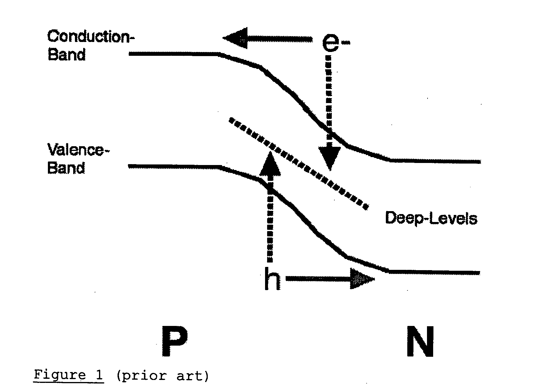
Conventional behavior is illustrated in FIG. 1. In a conventional p-n junction, electron transport occurs through the conduction band, and hole transport occurs through the valence band. (This transport through a conventional p-n junction is indicated by the solid arrows.) In a conventional p-n junction, deep-levels act as nonradiative recombination centers. (This is indicated by the dotted arrows, which show the trapping by deep-levels of electrons from the conduction band and holes from the valence band.)

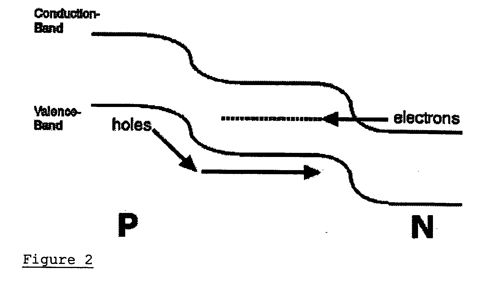
FIG. 2 shows a band diagram for an exemplary deep-level optical emitter. In this device, an optical transition occurs between the deep-level (indicated by the dashed line) and the valence-band. Electrons are injected into the deep-level from the n-type region, whereas holes are injected from the p-type region into the optically-active central region.

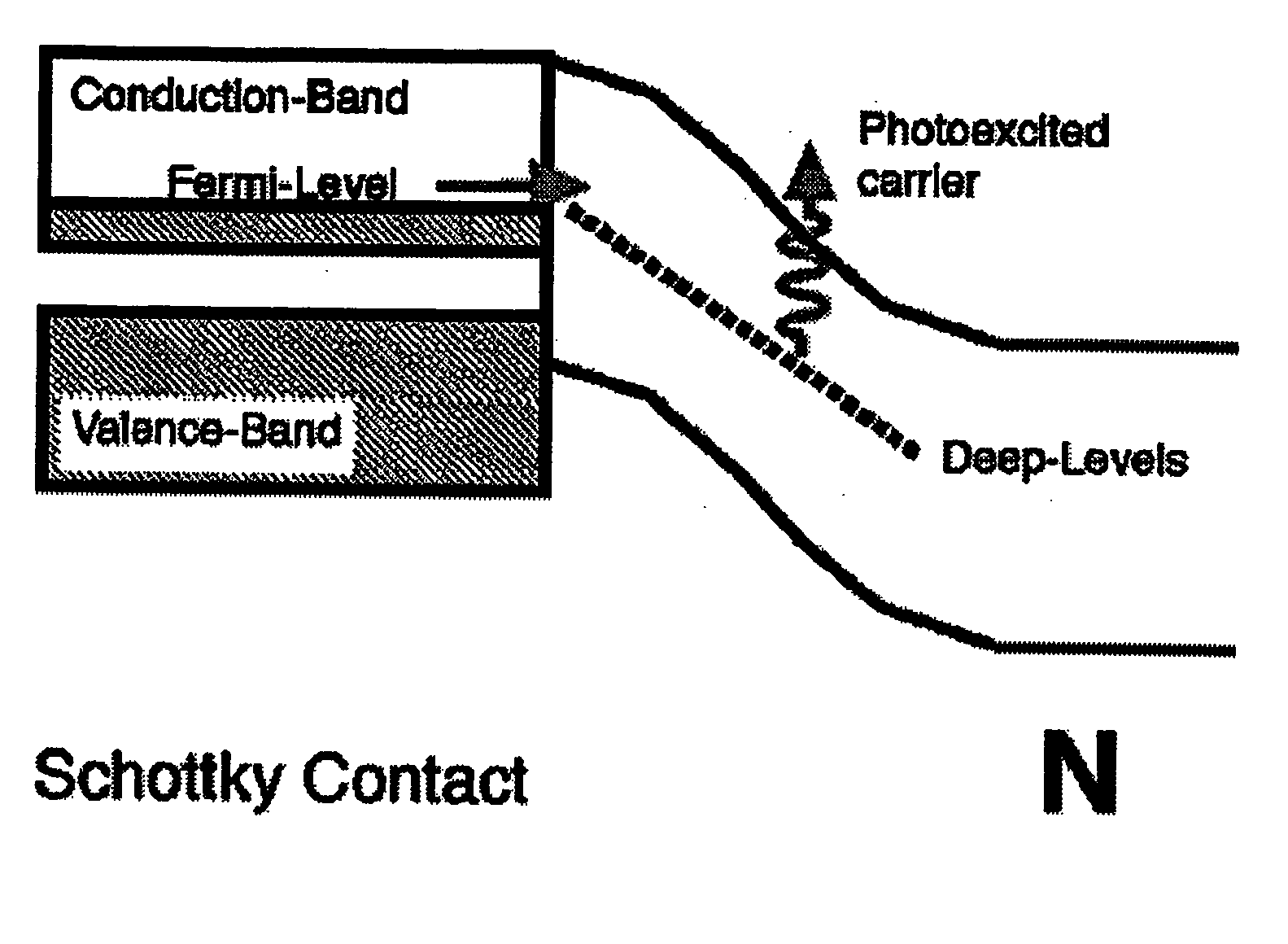
In FIG. 3, the efficiency of the deep-level optical emitter is improved through the addition of a Schottky contact carrier-inject...


PUM

PropertyMeasurementUnit
valence-band energyaaaaaaaaaa
conduction-band energyaaaaaaaaaa
energy gapaaaaaaaaaa

Abstract

The invention relates to the design, fabrication, and use of semiconductor devices that employ deep-level transitions (i.e., deep-level-to-conduction-band, deep-level-to-valence-band, or deep-level-to-deep-level) to achieve useful results. A principal aspect of the invention involves devices in which electrical transport occurs through a band of deep-level states and just the conduction band (or through a deep-level band and just the valence band), but where significant current does not flow through all three bands. This means that the deep-state is not acting as a nonradiative trap, but rather as an energy band through which transport takes place. Advantageously, the deep-level energy-band may facilitate a radiative transition, acting as either the upper or lower state of an optical transition.

Description

FIELD OF THE INVENTION The present invention relates generally to the field of semiconductor materials and devices, and more specifically to semiconductor materials and devices having an “artificial” energy band comprised of deep-level states. BACKGROUND OF THE INVENTION All semiconductor materials are characterized by an energy gap (EG) greater than zero. The energy gap is defined as the difference between the conduction-band edge (EC) and the valence-band edge (EV). A deep-level state is defined as a state having an energy level at least 0.05 EG above the valence-band edge and at least 0.05 EG below the conduction-band edge. A deep-level state can arise from a bound state of a substitutional impurity, an antisite, a vacancy on a lattice-site, an interstitial impurity, a dislocation, or a complex comprised of two or more deep-centers. For decades, semiconductor device designers have viewed deep-level states as something to be avoided, as their presence can degrade the performanc...

Claims


Application Information

Patent Timeline
Patent Type & Authority Applications(United States)
IPC IPC(8): H01L27/10H01L33/06H01S5/042H01S5/30H01S5/323
CPCH01L33/06H01S5/0421H01S5/0422H01S5/32316H01S5/3068H01S5/3086H01S5/30
Inventor PAN, JANET L.
Owner YALE UNIV
Why Eureka
Try Eureka