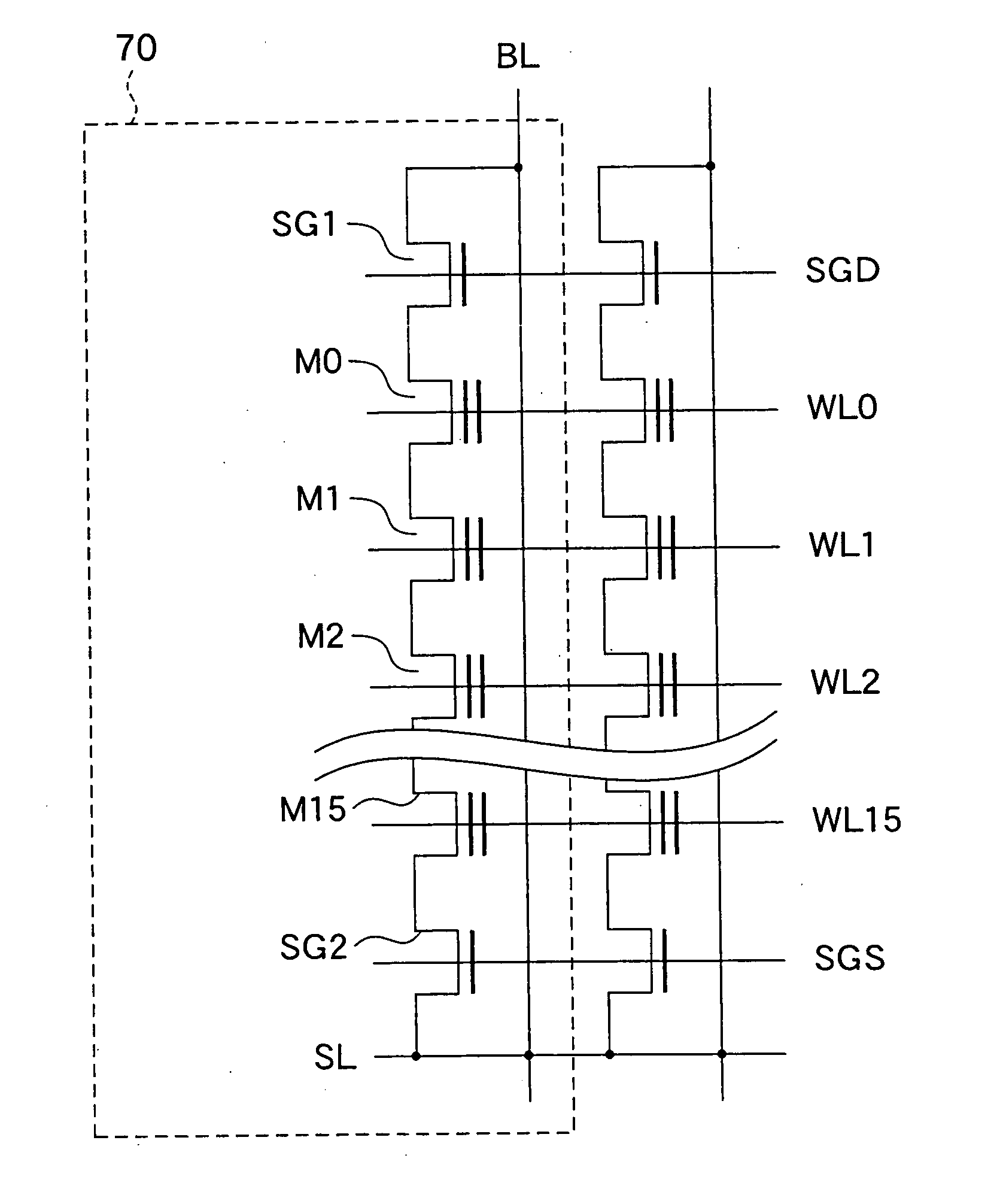
Nonvolatile semiconductor memory cell matrix, a mehtod for operating the same, monolithic integrated circuits and systems
- Summary
- Abstract
- Description
- Claims
- Application Information
AI Technical Summary
Benefits of technology
Problems solved by technology
Method used
Image

Examples
embodiments
[0093] The nonvolatile semiconductor memory includes a memory cell transistor, or memory cell transistors having an electric charge storage layer, so as to provide an enhancement mode transistor. The enhancement mode transistor functions as a select gate transistor by applying a functional select gate control signal to a word line connected thereto, so as to inject electric charges into the electric charge storage layer. A functional select gate control circuit is connected with the word line connected to the memory cell transistor, which functions as a select gate transistor. The functional select gate control circuit generates the functional select gate control signal.
[0094] The present invention relates to a NAND nonvolatile semiconductor memory cell matrix having a structure that has a floating gate at a charge storage layer, or a MONOS structure, and a NAND nonvolatile semiconductor memory system. By making the word lines of a memory cell array function as select gate lines, t...
first embodiment
[0108] In the first embodiment of the present invention, the circuitry, planar pattern structure, operation mode, element cross-section structure, manufacturing method, and matrix circuitry will be described centered on memory cell transistors functioning as select gate transistors. The number of select gate lines and / or transistors can be one, two, or three as required as long as the cutoff characteristic is ensured. In addition, different electrical potentials may be applied to the select gate lines and / or transistors, or for each group of a predetermined number of bit lines the select gate lines may be short-circuited so that the electrical potential is the same.
[0109] In the first embodiment of the present invention, by replacing some word lines in the memory cell array with select gate lines, the NAND flash memory can be made to operate by having the region surrounded by the select gate lines and / or transistors as the writing / erasing unit. First, writing by injecting electric ...
ninth modified example
of the First Embodiment
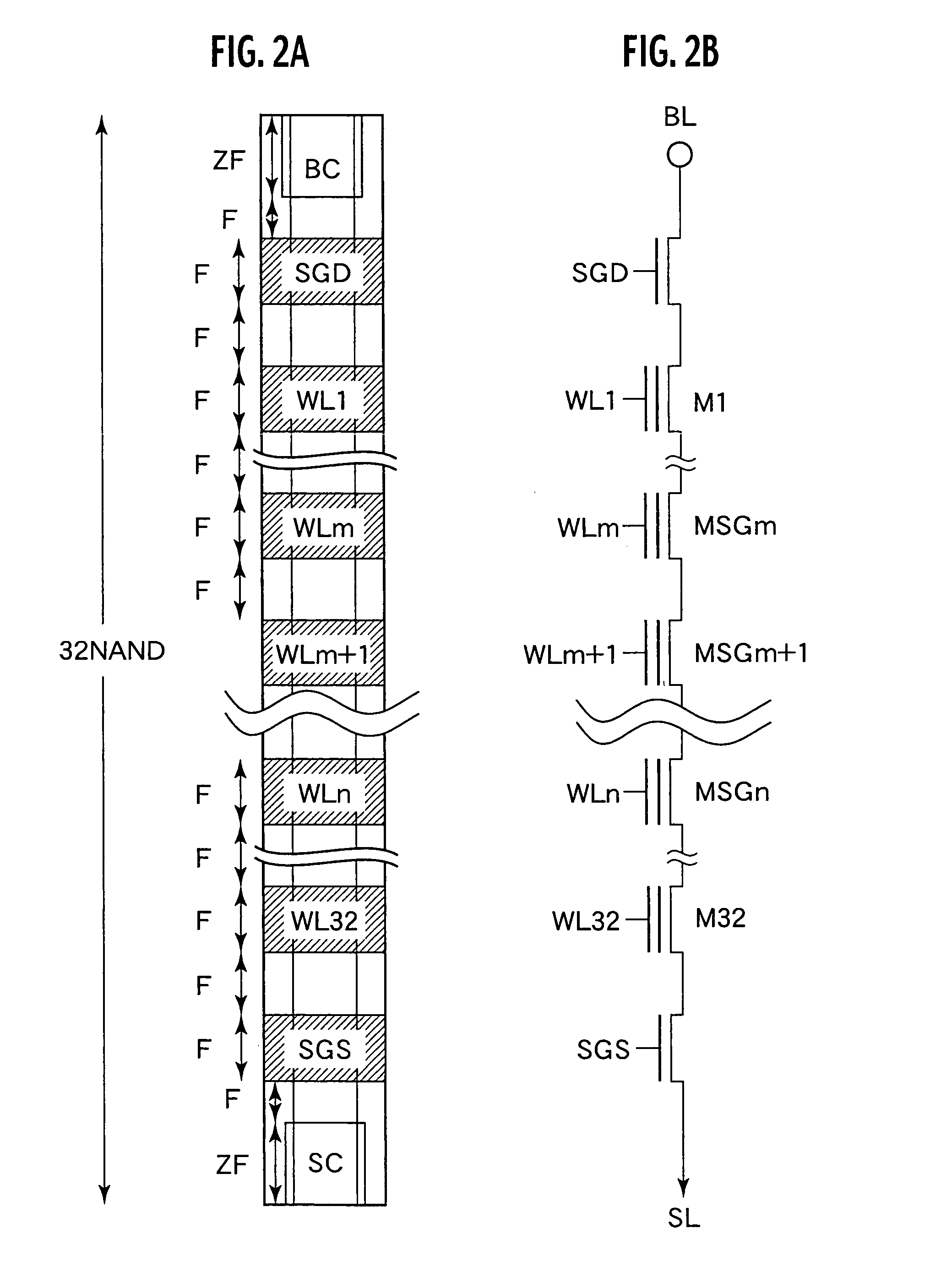
[0186] (Planar Pattern of Matrix Structure)
[0187]FIG. 17 is a planar form of a plurality of memory cell units according to a ninth modified example of the first embodiment of the present invention. FIG. 17 shows an example in which, of the memory cell transistors forming the NAND string, memory cell transistors corresponding to word lines WLm, WLn constitute memory cell transistor rows MSGm, MSGn functioning as select gate lines.
[0188] As shown in FIG. 17, select gates 21j, 21j are elongated in the row direction and are disposed parallel to each other in the column direction. Here, a plurality of memory cell transistors has the same gate length W1. Note that the plurality of memory cell transistors in a NAND string 23j−1, 23j, 23j+1 may consist of a number such as eight or sixteen. Furthermore, the pairs of select gates 21j, 21j arranged on both sides of the NAND string 23j−1, 23j, and 23j+1 have the same gate length W2. The gate length W2 may be equal to or...
PUM
 Abstract
Description
Claims
Application Information
 - R&D Engineer
- R&D Manager
- IP Professional
- Industry Leading Data Capabilities
- Powerful AI technology
- Patent DNA Extraction
Browse by: Latest US Patents, China's latest patents, Technical Efficacy Thesaurus, Application Domain, Technology Topic.
© 2024 PatSnap. All rights reserved.Legal|Privacy policy|Modern Slavery Act Transparency Statement|Sitemap