Stereolithographic method for forming insulative coatings for via holes in semiconductor devices, insulative coatings so formed, systems for forming the insulative coatings, and semiconductor devices including via holes with the insulative coatings

a technology of conductive metal and insulative coating, which is applied in the field of stereolithographic methods, can solve the problems of unsuitable cleaning equipment for use with relatively delicate structures, lack of machine vision systems, and difficulty in filling high aspect ratio via holes with conductive metals, so as to reduce the amount of unconsolidated materials

Inactive Publication Date: 2005-03-17
MICRON TECH INC
View PDF8 Cites 31 Cited by
  • Summary
  • Abstract
  • Description
  • Claims
  • Application Information

AI Technical Summary

Benefits of technology

[0039] A system according to the present invention includes an aperture-forming element, a dielectric material-introducing element, and a material consolidation element. The inventive system may also include one or both of an unused material-removal element and a conductive material introduction element. The aperture-forming element, which may comprise a router, a mechanical drill, a laser drill, or the like, is configured to form at least one precursor hole or other aperture in a substrate. The dielectric material-introducing element, which may comprise elements of a stereolithographic fabrication tank, a dispense needle, or the like, is configured to introduce unconsolidated dielectric material into the precursor hole or other aperture. The material consolidation element, which may comprise a stereolithographic material consolidati...

Problems solved by technology

As such, conventional stereolithographic apparatus lack machine vision systems for ensuring that structures are fabricated at certain locations.
Moreover, conventional stereolithographic apparatus lack support systems, handling systems, and cleaning equipment which are suitable for use with relatively delicate structures, such as semiconductor substrates and semiconductor devices that have been fabricated thereon.
While higher circuit densities are possible where the via hole diameter is very small, suitably filling high aspect ratio via holes with a conductive metal is difficult.
Oxidation or adhesion promotion of the inner surfaces of the precursor hole is required because adhesion of polymer directly to silic...

Method used


Image

  • Stereolithographic method for forming insulative coatings for via holes in semiconductor devices, insulative coatings so formed, systems for forming the insulative coatings, and semiconductor devices including via holes with the insulative coatings
  • Stereolithographic method for forming insulative coatings for via holes in semiconductor devices, insulative coatings so formed, systems for forming the insulative coatings, and semiconductor devices including via holes with the insulative coatings
  • Stereolithographic method for forming insulative coatings for via holes in semiconductor devices, insulative coatings so formed, systems for forming the insulative coatings, and semiconductor devices including via holes with the insulative coatings

Examples


Embodiment Construction

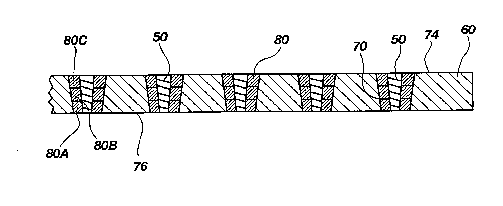
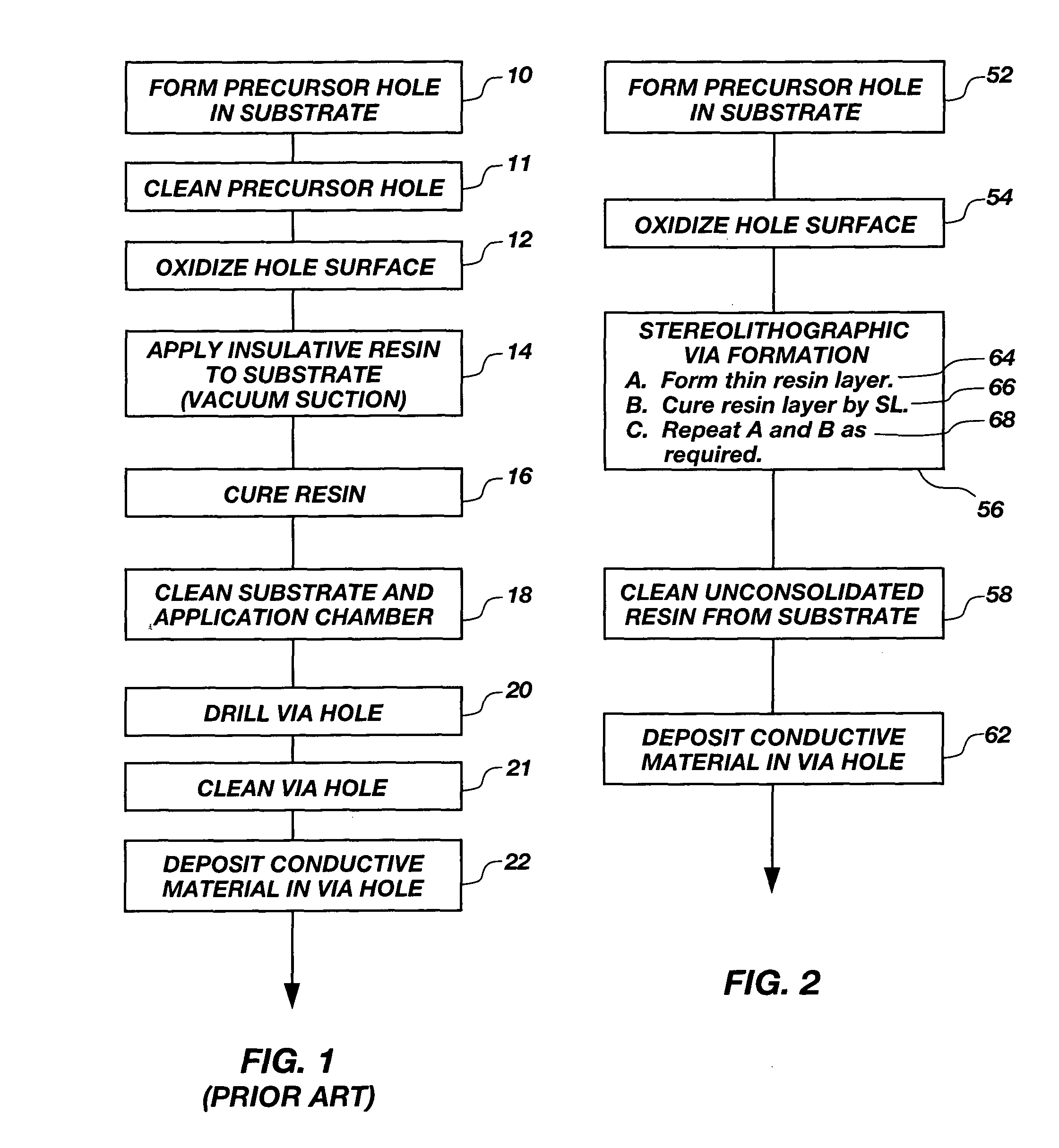
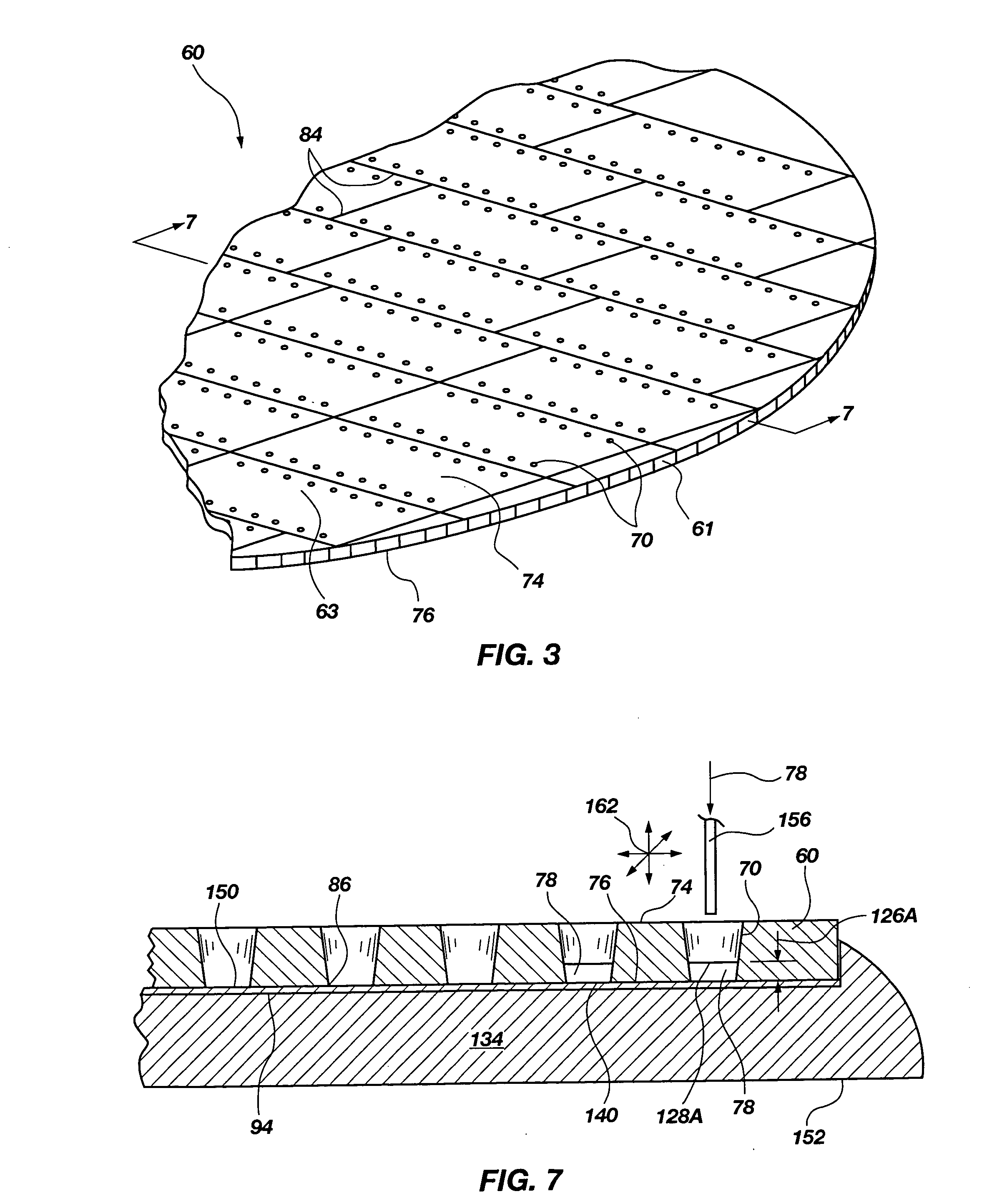
[0059] Turning now to the present invention, an exemplary method is outlined in FIG. 2 and illustrated in the remaining figures. The method is useful for lining one or more apertures, such as precursors to via holes 50 (FIG. 13), or “precursor holes”70 (FIG. 8), formed in a substrate 60 with an insulative coating 80 to prevent shorting of conductive vias that are subsequently formed in the via holes. As shown in FIG. 3, substrate 60 may be a full or partial wafer of semiconductive material (e.g., silicon, gallium arsenide, indium phosphide), another large-scale substrate, such as an SOI-type substrate, an insulative substrate (e.g., glass, ceramic, etc.), an electrically conductive material, a flexible or rigid circuit board, an individual interposer or collection of individual interposers, an individual semiconductor device or collection of individual semiconductor devices, or the like. The exemplary substrate 60 shown in FIG. 3 comprises a multichip wafer 61 containing many unsing...


PUM

PropertyMeasurementUnit
Dielectric polarization enthalpyaaaaaaaaaa
Electrical conductivityaaaaaaaaaa
Volumeaaaaaaaaaa

Abstract

A method for forming insulating precursors to via holes formed through conductive and semiconductive substrates includes use of stereolithographic processes. An unconsolidated material is introduced into a precursor hole, then regions of the unconsolidated material that are located adjacent to the surface of each precursor hole are selectively consolidated to form an insulative coating thereon. This process may be conducted once to form a single-layered insulative coating or multiple times to form multilayered insulative coatings. Subsequently, unconsolidated material may be removed to expose a via hole that extends through the insulative coating. Structures that include via holes and conductive vias that have been insulated in this manner are also disclosed, as are systems for forming the insulative coatings.

Description

BACKGROUND OF THE INVENTION [0001] 1. Field of the Invention [0002] The present invention relates generally to processes and methods for forming electronic devices and the like. More particularly, the present invention pertains to methods and apparatus for effecting the creation of via holes in semiconductors and other thin substrates and, more specifically, to methods and apparatus for forming insulative coatings of via holes. The present invention also pertains to the use of stereolithography techniques to form insulative coatings with small diameter via holes extending therethrough. [0003] 2. Background of Related Art [0004] Over the past decade or so, a manufacturing technique which has become known as “stereolithography” and which is also known as “layered manufacturing” has evolved to a degree where it is employed in many industries. [0005] Basically, stereolithography, as conventionally practiced, involves utilizing a computer, typically under control of three-dimensional (3-...

Claims


Application Information

Patent Timeline
IPC IPC(8): G03F7/00H01L21/48H01L21/68H01L21/768H01L23/48H01L23/498H05K3/00H05K3/44
CPCB29C67/0055B29C67/0066H01L2924/0002G03F7/0037H01L21/486H01L21/6835H01L21/76831H01L21/76898H01L23/49827H01L2221/68345H01L2221/6835H01L2223/6622H01L2924/09701H05K3/0023H05K3/0082H05K3/445H05K2203/107H05K2203/1476H01L2924/00B29C64/135B29C64/106H01L21/4763
Inventor FARNWORTH, WARREN M.
Owner MICRON TECH INC
Why Eureka
Try Eureka