
Near-field light generating structure, near-field exposure mask, and near-field generating method

a near-field light and generating structure technology, applied in the field of near-field light generating structure, near-field exposure mask, near-field generating method, and near-field recording and reproducing an apparatus, can solve the problems of weak electric field generation, shortening the wavelength of laser light, and low throughput, so as to achieve efficient generation

Inactive Publication Date: 2005-03-24
CANON KK
View PDF13 Cites 38 Cited by
  • Summary
  • Abstract
  • Description
  • Claims
  • Application Information

AI Technical Summary

Benefits of technology

An object of the present invention is to provide a near-field exposure mask permitting efficient generation of intense near-field light at a desired position, and its manufacturing method.
According to the first aspect of the present invention, it is possible to realize a near-field exposure mask which permits generation of near-field light at a high efficiency and is capable of generating intense near-field light at a desired position, a near-field light generating method, a near-field exposure mask manufacturing method, a near-field generating method, a near-field exposure mask manufacturing method, a near-field exposure apparatus, a near-field exposure method, and a microdevice manufacturing method. Further, it is possible to suppress a lateral expanse of near-field light generation area. Accordingly, it becomes possible to perform a high-resolution exposure in a short time.

Problems solved by technology

While the fineness is being improved in the optical lithography, in order to assure microprocessing of 0.1 μm or narrower, there still remain many unsolved problems such as further shortening of wavelength of laser light, development of lenses usable in such wavelength region, and the like.
Thus, there is a problem that the throughput is not high.
Further, it is difficult to generate a strong electric field at a desired position, so that a desired exposure pattern is not necessarily obtained satisfactorily.

Method used


Image

  • Near-field light generating structure, near-field exposure mask, and near-field generating method
  • Near-field light generating structure, near-field exposure mask, and near-field generating method
  • Near-field light generating structure, near-field exposure mask, and near-field generating method

Examples


embodiment 1

FIGS. 3(a) to 3(f) are sectional views for illustrating production steps of a near-field exposure mask manufacturing method in this embodiment.

First of all, a substrate 301 of Si wafer with (100) plane is prepared. On each of both surfaces of the substrate 301, a 500 nm-thick silicon nitride layer is formed as a base material 302 (FIG. 3(a)).

Next, a back-etching opening 303 is formed is a pattern on the light-incident side surface of the base material 302 through lithography. On the light-outgoing side surface of the base material 302, a 50 nm-thick light blocking metal layer 304 of Cr is formed (FIG. 3(b)).

Then, on the light blocking metal layer 304, an etching mask layer (not shown) is formed and patterned in a slit array shape by using an EB drawing apparatus and a dry etching apparatus. Thereafter, a fine pattern 305 is formed in the light blocking metal layer 304 and the etching mask layer is removed (FIG. 3(c)). The patterning may also be performed through other methods...

embodiment 2

FIGS. 4(a) to 4(c) are sectional views for illustrating production steps of a near-field exposure mask manufacturing method in this embodiment.

First, a substrate 401 of Si wafer with (100) plane is prepared. On each of both surfaces of the substrate 401, a 500 nm-thick silicon nitride layer is formed as a base material 402 (FIG. 4(a)).

Next, a back-etching opening 403 is formed in a pattern on the light-incident side surface of the base material 402 through lithography. On the light-outgoing side surface of the base material 402, a 50 nm-thick light blocking metal layer 404 of Cr is formed (FIG. 4(b)).

Then, the light blocking metal layer 404 is subjected to patterning with focused ion beam 406. At that time, the light blocking metal layer 404 is formed in an asymmetrical shape by obliquely irradiating the substrate with the focused ion beam 406. Thereafter, in a KOH aqueous solution, anisotropic etching of the resultant structure is performed to prepare a near-field exposure m...

embodiment 3

FIGS. 6(a) to 6(d) are sectional views for illustrating production steps of a near-field exposure mask manufacturing method in this embodiment.

First, a substrate 601 of Si wafer with (100) plane is prepared. On each of both surfaces of the substrate 601, a 500 nm-thick silicon nitride layer is formed as a base material 602 (FIG. 6(a)).

Next, a back-etching opening 603 is formed in a pattern on the light-incident side surface of the base material 602 through lithography. On the light-outgoing side surface of the base material 602, a 50 nm-thick light blocking metal layer 604 of Cr is formed (FIG. 6(b)).

Onto the light blocking metal layer 604, a photoresist 605 is applied and subjected to patterning (FIG. 6(c)). During the patterning, the photoresist may preferably be exposed obliquely to light with respect to the substrate so as to provide an angle suitable for a subsequent step of performing oblique dry etching. Then, the dry etching is performed with respect to the substrate ...


PUM


Abstract

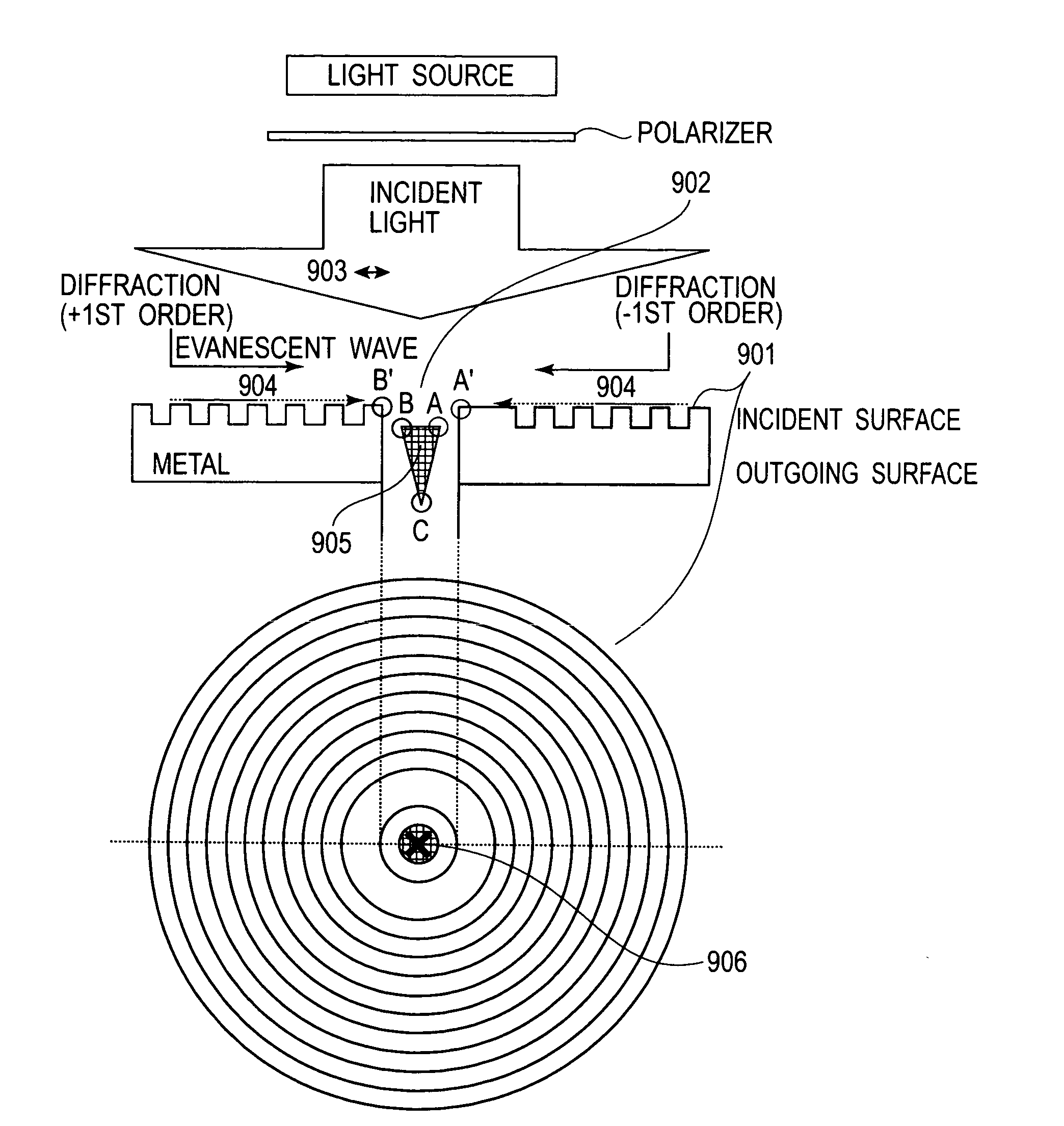
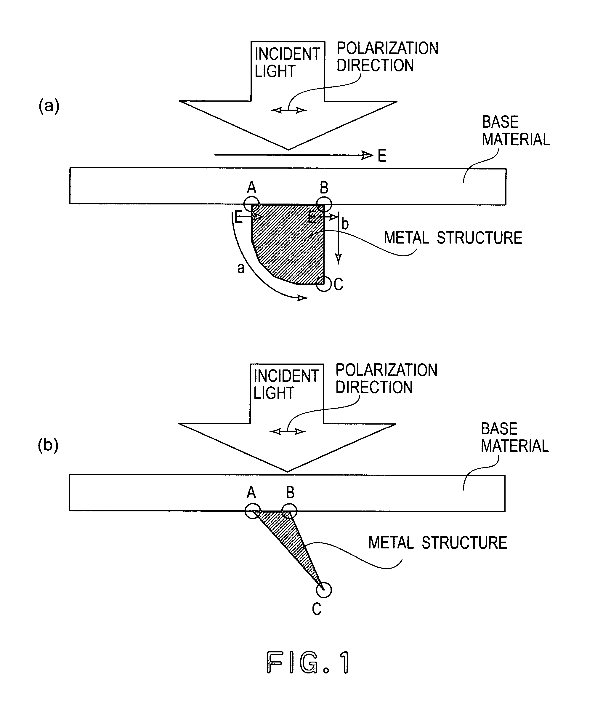
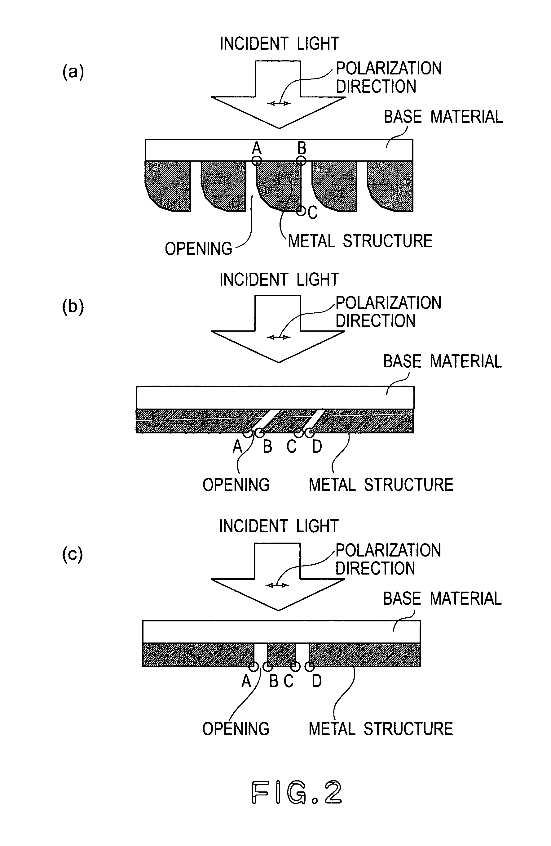
A near-field light generating structure for generating near-field light has a pattern of a fine metal structure comprising a light blocking layer or a pattern of a fine opening provided in the light blocking layer. The fine metal structure or the fine opening has a size of not more than a wavelength of incident light. The fine metal structure or the fine opening has a sectional shape, in a plane parallel with the incident light, which is asymmetrical in terms of a member adjacent to the fine metal structure or the fine opening.

Description

FIELD OF THE INVENTION AND RELATED ART The present invention relates to a near-field light generating structure, a near-field exposure mask, a near-field generating method, and a near-field recording and reproducing an apparatus. Increasing capacity of a semiconductor memory and increasing speed and density of a CPU processor have inevitably necessitated further improvements in fineness of microprocessing through optical lithography. Generally, the limit of microprocessing with an optical lithographic apparatus is of an order of the wavelength of light used. Thus, the wavelength of light used in optical lithographic apparatuses has been shortened more and more. Currently, near ultraviolet laser is used, and microprocessing of 0.1 μm order is enabled. While the fineness is being improved in the optical lithography, in order to assure microprocessing of 0.1 μm or narrower, there still remain many unsolved problems such as further shortening of wavelength of laser light, development ...

Claims


Application Information

Patent Timeline
IPC IPC(8): G03C5/04G03F1/08G03F1/14G03F9/00H01J3/14
CPCG03F1/54G03F1/14G03F1/50
Inventor YAMADA, TOMOHIROKURODA, RYOMIZUTANI, NATSUHIKO
Owner CANON KK
Learn More