Microfabricated structures and processes for manufacturing same

a microfabricated structure and mold technology, applied in microstructural technology, microelectromechanical systems, microelectroforming processes, etc., can solve the problems of serial processing, high cost of devices, and many limitations of the surface exposed to fluids and/or biological samples, so as to minimize the roughness of the surface of the microstructure

Inactive Publication Date: 2005-03-31
CINCINNATI UNIVERISITY OF THE
View PDF11 Cites 179 Cited by
  • Summary
  • Abstract
  • Description
  • Claims
  • Application Information

AI Technical Summary

Benefits of technology

[0018] Disclosed herein is an embodiment of a two-step electroplating technique, wherein the height of the microstructures on the master mold is controlled precisely using a polishing step after electroplating of the microstructures. The structural integrity of the microstructures is preserved by the use of a second sacrificial support metal which is also electroplated, following the first electroplating step. The s

Problems solved by technology

However, specifically for microfluidic and more specifically for BioMEMS related applications, Silicon and Glass were observed to have many limitations in terms of the surface exposed to the fluids and/or biological samples.
One specific problem is non-specific adsorption of proteins commonly encountered in biological samples.
With the high intrinsic cost of these substrates, the serial processing further adds to the cost of the device.
However, Silicon master-mold cannot be easily used with injection molding equipment due to processing complexities and the relatively fragile nature of the Silicon substrate.
Hot embossing is an inherently slow-process and cannot match the short-cycle times of injection molding.
However, the milling process is limited in terms of achievable feature size and aspect ratio (the ratio of height to width for a microstructure).
One of the difficulties in this method is the fabrication of structures that do not have a rectangular cross-section.
Another major drawback in UV-LIGA based master mold fabrication is non-uniform electroplating thickness in photoresist mold patterns having different dimensions (specifically different widths).
This may give rise to problems where the microstructure needs to be very accurately defined e.g. in microfluidic applications.
Furthermore, another problem of the current-crowding effect is the non-uniform cross-sectional profile achieved after electroplating, wherein typically (along t

Method used


Image

  • Microfabricated structures and processes for manufacturing same
  • Microfabricated structures and processes for manufacturing same
  • Microfabricated structures and processes for manufacturing same

Examples


Embodiment Construction

”.

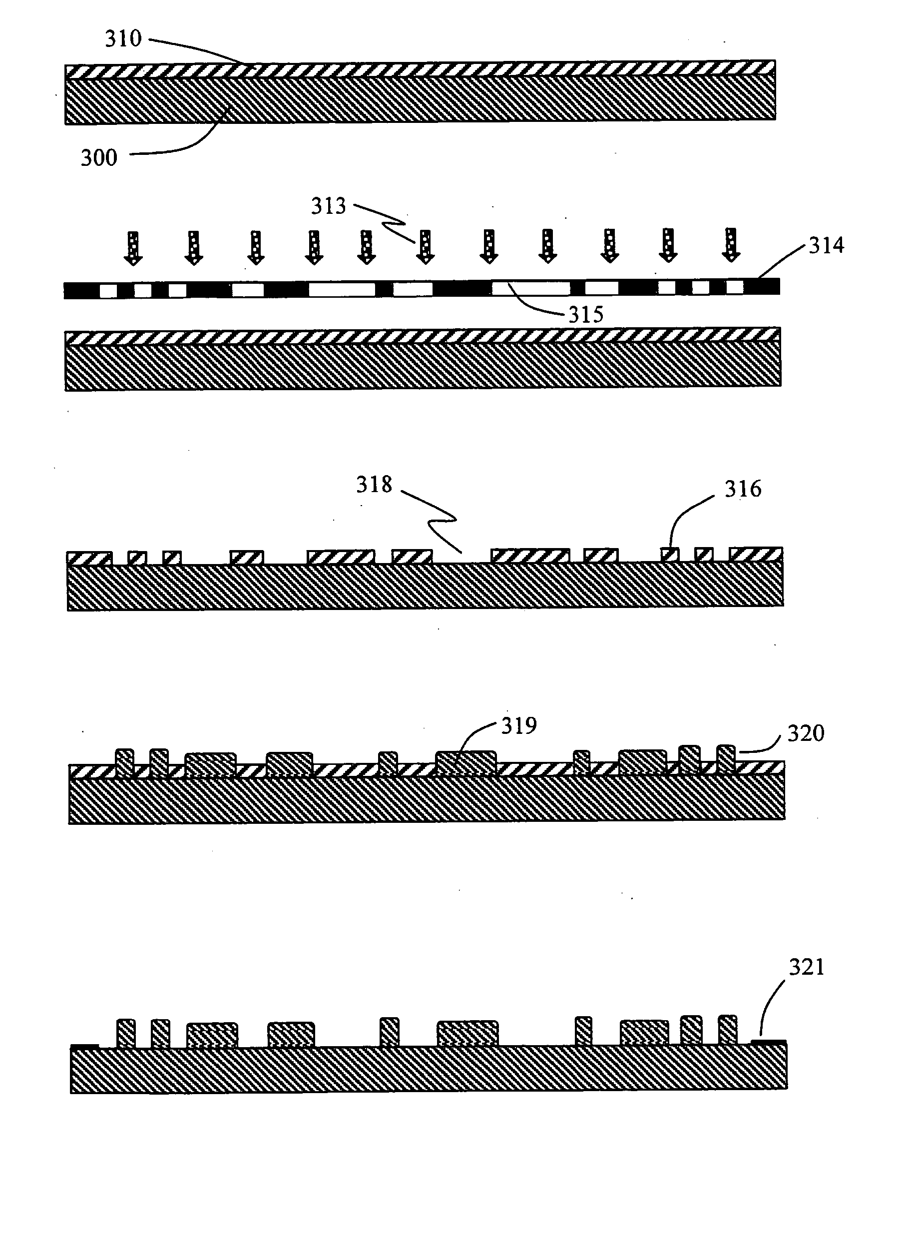
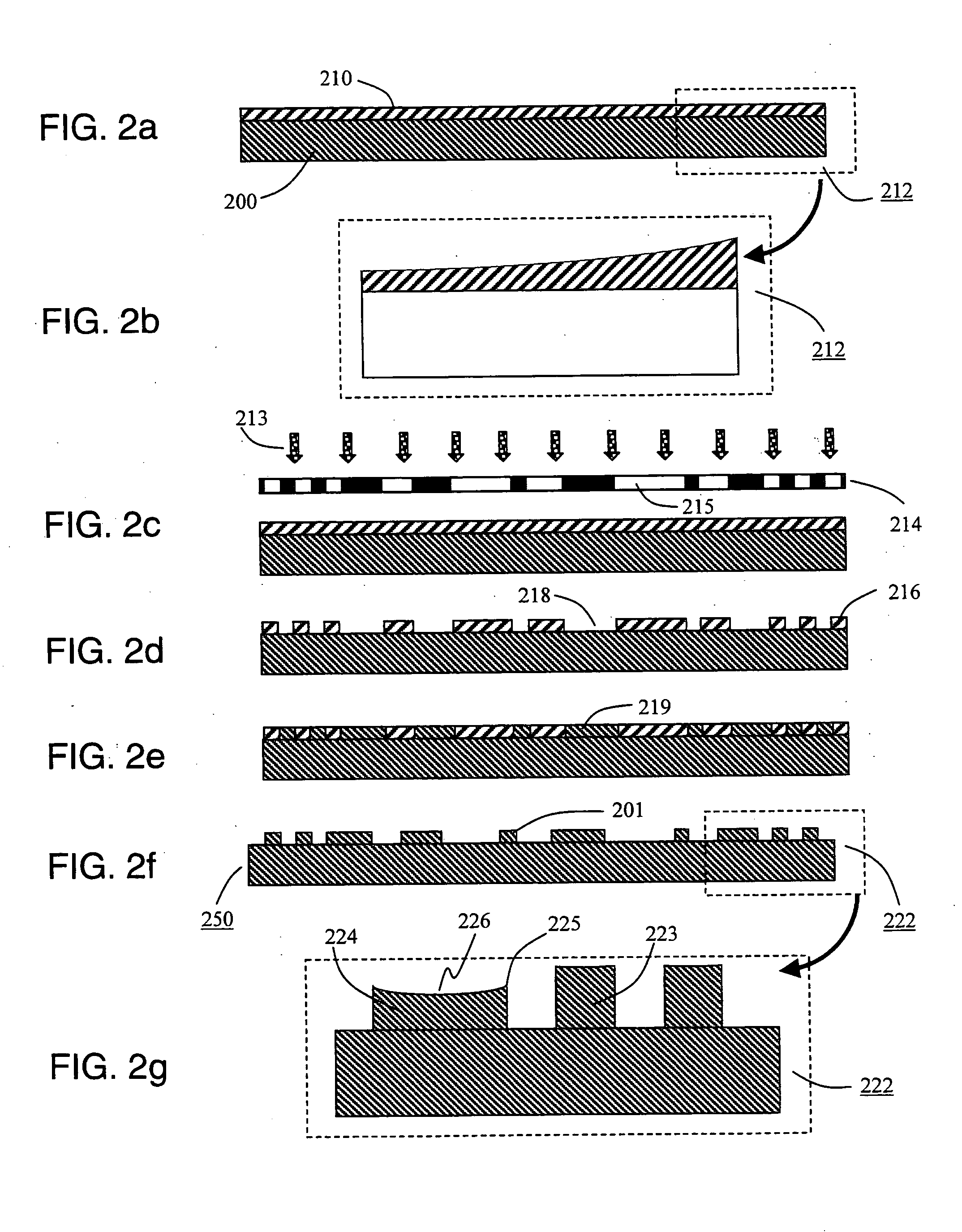
[0020] Certain embodiments of the present invention provide an elegant solution to creating a negative image of an array of Piano-Convex microlenses on a master mold and subsequently replicating the Plano-Convex lens array structure on the plastic substrate.

[0021] Embodiments of the present invention overcome the deficiencies and inadequacies in the prior art as described in the previous section and as generally known in the industry.

[0022] Certain embodiments of the present invention are concerned with developing a master mold for plastic replication, wherein the master mold is a discrete component, which can be easily assembled into the injection mold block for plastic replication.

[0023] Certain embodiments of the present invention are concerned with developing a master mold using a modified UV-LIGA fabrication process, specifically the two-step electroplating process with one of the electroplating used for sacrificial metal deposition, to create master molds with microstruct...


PUM

PropertyMeasurementUnit
Concentrationaaaaaaaaaa
Structureaaaaaaaaaa
Microstructureaaaaaaaaaa

Abstract

Various techniques for the fabrication of highly accurate master molds with precisely defined microstructures for use in plastic replication using injection molding, hot embossing, or casting techniques are disclosed herein. Three different fabrication processes used for master mold fabrication are disclosed wherein one of the processes is a combination of the other two processes. In an embodiment of the first process, a two-step electroplating approach is used wherein one of the metals forms the microstructures and the second metal is used as a sacrificial support layer. Following electroplating, the exact height of the microstructures is defined using a chemical mechanical polishing process. In an embodiment of the second process, a modified electroforming process is used for master mold fabrication. The specific modifications include the use of Nickel-Iron (80:20) as a structural component of the master mold, and the use of a higher saccharin concentration in the electroplating bath to reduce tensile stress during plating and electroforming on the top as well as sides of the dummy substrate to prevent peel off of the electroform. The electroforming process is also well suited towards the fabrication of microstructures with non-rectangular cross sectional profiles. Also disclosed is an embodiment of a simple fabrication process using direct deposition of a curable liquid molding material combined with the electroforming process. Finally, an embodiment of a third fabrication process combines the meritorious features of the first two approaches and is used to fabricate a master mold using a combination of the two-step electroplating plus chemical mechanical polishing approach and the electroforming approach to fabricate highly accurate master molds with precisely defined microstructures. The microstructures are an integral part of the master mold and hence the master mold is more robust and well suited for high volume production of plastic MEMS devices through replication techniques such as injection molding.

Description

CROSS-REFERENCE TO RELATED APPLICATIONS / INCORPORATION BY REFERENCE [0001] This application claims priority to provisional U.S. Patent Applications Ser. Nos. 60 / 506,641; 60 / 506,226; 60 / 506,321; 60 / 506,424; and 60 / 506,635 all filed on Sep. 26, 2003, and all of which are incorporated herein by reference in their entirety.GOVERNMENT SUPPORT [0002] The U.S. Government has a paid-up license in this invention and the right in limited circumstances to require the patent owner to license others on reasonable terms as provided for by the terms of grant no. AF F30602-00-1-0569 awarded by the Defense Advanced Research Projects Agency (DARPA).[0003] This patent application is being filed concurrently with U.S. Patent Applications having attorney docket numbers 200057.00008, 200057.00009, 200057.00010, and 200057.00011, which are incorporated herein by reference in their entirety. TECHNICAL FIELD [0004] Embodiments of the present invention generally relate to the fabrication of ultra-high precisi...

Claims


Application Information

Patent Timeline
IPC IPC(8): C25D1/10
CPCB81B2203/033B81B2203/0361C25D1/10B81C99/009B81B2203/0376
Inventor AHN, CHONG H.TRICHUR, KRISHNANAPPASAMY, SREERAM C.
Owner CINCINNATI UNIVERISITY OF THE
Why Eureka
Try Eureka