Contact printing using a magnified mask image

a technology of contact printing and mask image, which is applied in the direction of microlithography exposure apparatus, photomechanical treatment, instruments, etc., can solve the problems of affecting the quality of contact printing, so as to prevent the adhesion of the lens element

Inactive Publication Date: 2005-03-31
APPLIED MATERIALS INC
View PDF8 Cites 702 Cited by
  • Summary
  • Abstract
  • Description
  • Claims
  • Application Information

AI Technical Summary

Benefits of technology

In yet other embodiments of the invention, the method includes preventing adhesion of the lens element to the layer.

Problems solved by technology

Since the mask image and the wafer image are of the same dimension, this technique was partially abandoned for volume manufacturing because of the tight requirements on the mask image and the difficulty to obtain good contact over the entire wafer area.
As the feature size decreases, distortion in the pattern transfer process becomes more severe.
In the case of OPC, modifications of the design image account for optical limitations as well as mask fabrication limitations and resist limitations.
The destructive interference between adjacent regions of opposite phase creates a very sharp contrast at the boundary between the regions, thus leading to the printing of small features on the wafer.
The main challenge of immersion lithography is the manufacturing of steppers and scanners capable of handling a film of liquid between the lens and the wafer without creating bubble or non-uniformities.
The addition of an immersion film could result in vibration coupling between the stage and the lens.
Another challenge is the limited availability of transparent liquids with a high refractive index at 193 nm or 157 nm.
The printing of dies at the edge of the wafer also represents a challenge for liquid immersion lithography.
Indeed, to image such a field size, the solid immersion lens would be too thick compared to the distance between the projection lens and the wafer.
Moreover the set up proposed is limited by aberrations when a large field is imaged.
These tight requirements make the use of two separate lenses as described in U.S. Pat. No. 5,121,256 impractical.
The drawback of this implementation is that the temperature of the resist needs to be increased during the imprint step and then decreased before the mold is removed thus leading to long processing time and possible distortion of the image due to thermal expansion.
The difficulty of making such an accurate pattern is one of the main limitations of nano-imprint lithography.

Method used


Image

  • Contact printing using a magnified mask image
  • Contact printing using a magnified mask image
  • Contact printing using a magnified mask image

Examples


Embodiment Construction

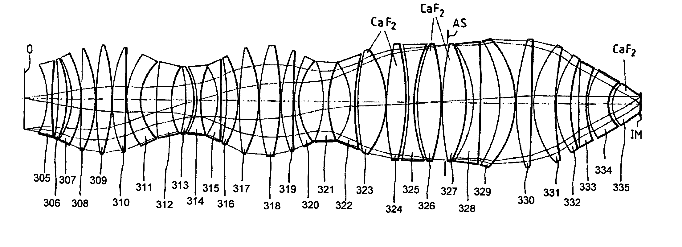
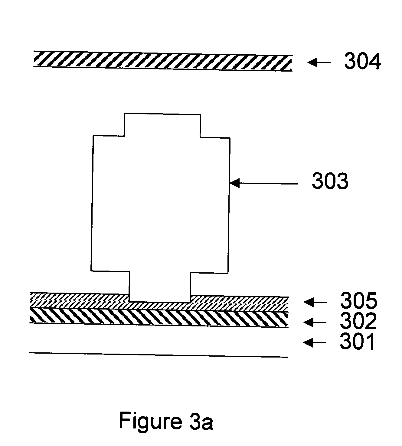
A technique described in FIG. 3a was developed to address the issues encountered with immersion lithography. A wafer 302, coated with a resist 305 is placed on the stage 301. The projection lens 303 projects an image of the mask 304 inside the resist 305. The resist layer is deformable so that the bottom surface of the lens is pushed inside the resist layer at a certain distance from the top of the nominal resist height. The depression in the resist can be obtained by displacement if the resist is a liquid or by compression if the resist is made of a deformable material. The quality of the contact between the lens and the resist is guaranteed by the fact that the lens is pushed inside the resist in a similar fashion as in the case of nano-imprint lithography. In this case, the absence of patterns at the surface of the lens or at the surface of the resist allows for a better contact with no gaps. Inserting an immersion lens as described in the U.S. Pat. No. 5,121,256 is not required ...


PUM

PropertyMeasurementUnit
wavelengthaaaaaaaaaa
wavelengthsaaaaaaaaaa

Abstract

Improvements in the fabrication of integrated circuits are driven by the decrease of the size of the features printed on the wafers. Current lithography techniques limits have been extended through the use of phase-shifting masks, off-axis illumination, and proximity effect correction. More recently, liquid immersion lithography has been proposed as a way to extend even further the limits of optical lithography. This invention described a methodology based on contact printing using a projection lens to define the image of the mask onto the wafer. As the imaging is performed in a solid material, larger refractive indices can be obtained and the resolution of the imaging system can be increased.

Description

FIELD OF THE INVENTION The invention relates to the process of fabricating semiconductor chips. More specifically, the invention relates to a lithographic method. RELATED ART Integrated circuit technology improvements are mostly driven by the decrease of the feature size of the semiconductor chips. As the feature size of the circuit decreases, circuit designers have to deal with the limitations of the lithography process used to manufacture the integrated circuits. The lithography process starts first by coating the surface of the semiconductor wafer with a material called resist. A source of radiation is then shone through the mask in the case of a transparent mask. For a reflective mask the radiation is reflected by the mask. The transparent mask is made of a substrate transparent to the radiation and coated with a patterned opaque layer defining clear and opaque regions to the radiation. Transparent masks are mostly used in optical lithography with typical wavelengths of 436 nm...

Claims


Application Information

Patent Timeline
Patent Type & Authority Applications(United States)
IPC IPC(8): G02B13/14G03F7/20
CPCG03F7/70241G02B13/143
Inventor PIERRAT, CHRISTOPHEWONG, ALFRED KWOK-KIT
Owner APPLIED MATERIALS INC
Why Eureka
Try Eureka