

Laser diode module, laser apparatus and laser processing apparatus
a laser processing and diode module technology, applied in semiconductor lasers, instruments, optical elements, etc., can solve the problems of shortening the service life, and reducing the efficiency of electric-to-light conversion
- Summary
- Abstract
- Description
- Claims
- Application Information
AI Technical Summary
Benefits of technology
Problems solved by technology
Method used
Image

Examples
example 1
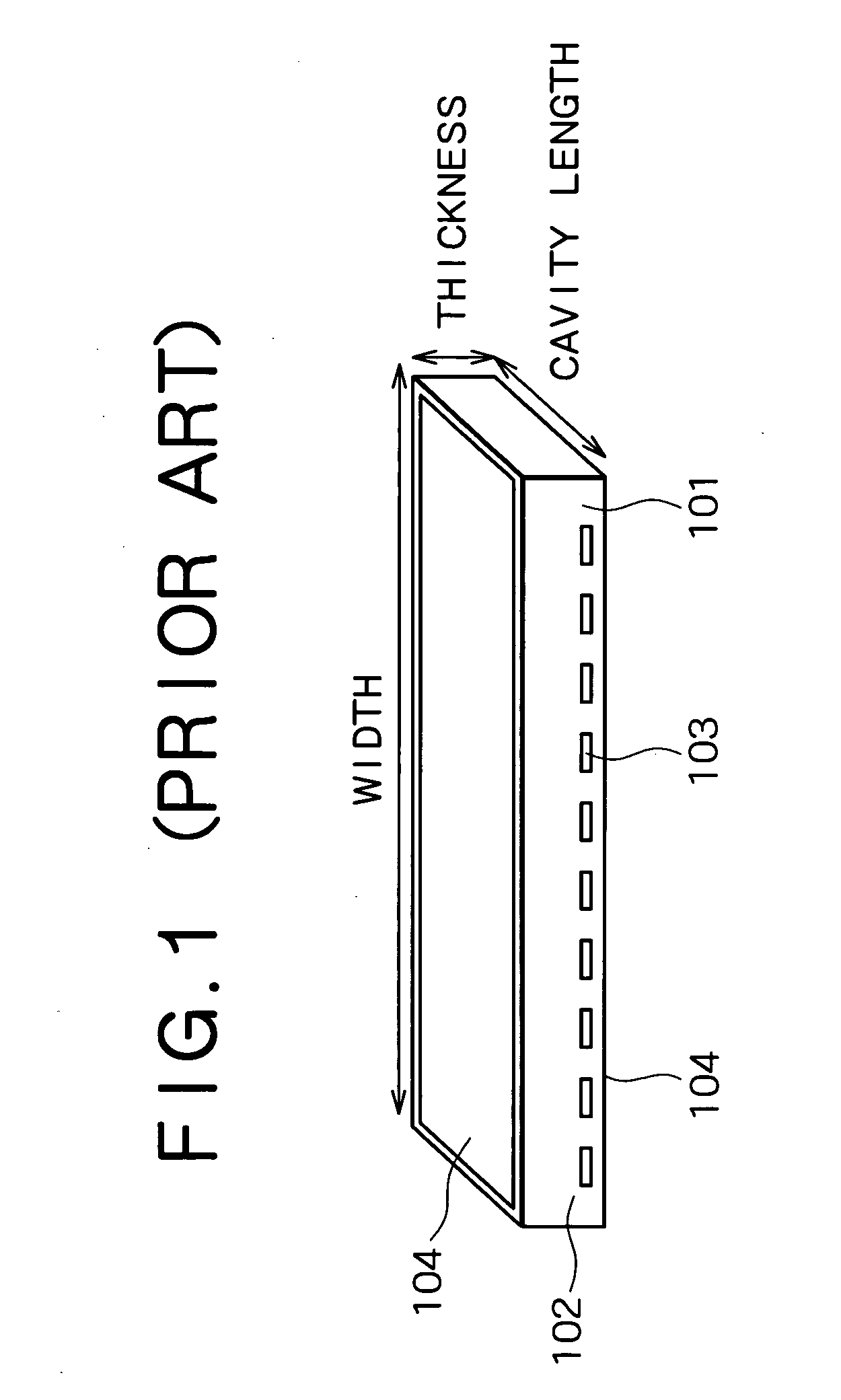
[0091] To demonstrate the effects of the invention, the characteristics of examples that fall within the scope of the invention and the characteristics of comparative examples which are out of the scope of the invention will be discussed. A laser diode array bar having a width of 10 mm, a cavity length of 1.2 mm and a thickness of 100 μm and capable of providing an output of 50 W and submount substrates formed of CuW having a width of 10 mm, a length of 1.2 mm and a thickness of 0.15 mm were prepared. A gold layer was formed 1 μm thick on the topmost surfaces of the upper and lower electrodes of the laser diode. Gold was plated 1 μm thick on the topmost surfaces of both submount substrates, and a gold-tin solder was deposited 2 μm thick on the other sides. After the laser diode bar was sandwiched by the two submount substrates with the gold-tin soft solder sides facing to the top and bottom sides of the laser diode bar in such a way that the light emission sides of the laser diode b...
example 2
[0098] The members similar to those of Example 1 were used, a nickel layer of 1 μm in thickness was deposited on the top surface of only the heat sink, and the life test of the laser diode module was conducted while changing the thickness of the In layer from 1 μm to 10 μm as per Example 1. With the same experiment as illustrated in FIG. 6 conducted, a failure probability became 0.1% or less when the thickness of the In layer was 30 μm or greater. This is because nickel, when used, shows slow alloying with In, thus providing the reliability with a thinner In solder as compared with the use of gold. Through the same experiment as illustrated in FIG. 12 conducted, an output of 50 W was obtained when the current of 64 A was let to flow in the module and the thermal resistance of the junction part was larger than that in case gold was used. However, there is an output drop ratio of about 10% over 10,000 hours as in the case of the gold layer, which apparently raises no practical problem...
example 3
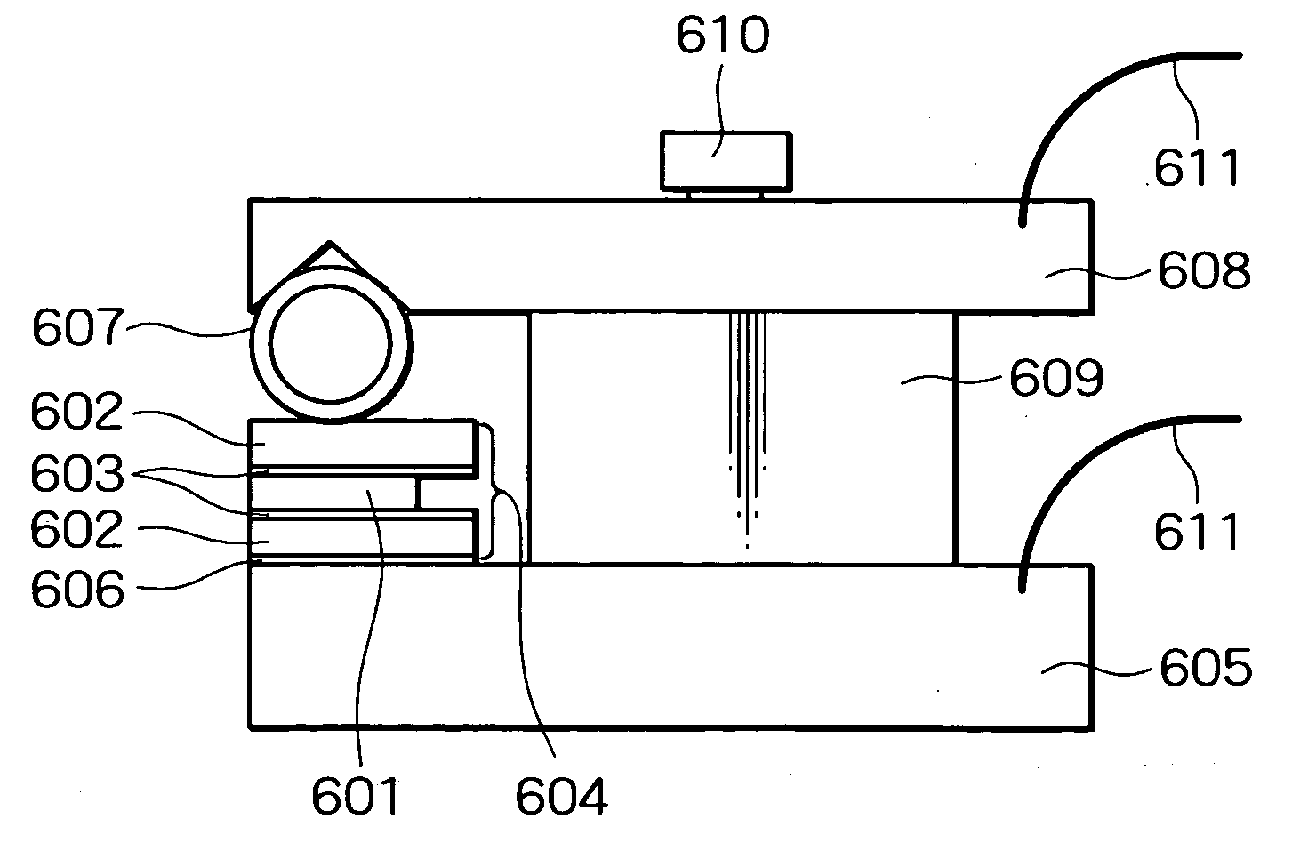
[0099]FIG. 20 is a perspective view showing an arrayed laser diode module according to Example 3 of the invention. The arrayed laser diode module has five laser diode modules prepared in Example 1 arranged sideways. A sandwiched assembly 2002 formed by a laser diode bar mounted on a heat sink 2001 and submount substrates, and a coil electrode 2003 in use were the same as those of Example 1, and the sandwiched assembly 2002 was mounted on the heat sink 2001 with the same soft solder. A holder 2004 formed of an insulator to let water flow to the five heat sinks 2001 was prepared, and the individual heat sinks were secured at predetermined positions of the holder 2004. Then, individual bridge presser electrodes 2005 were laid out as shown in FIG. 20. The four bridge presser electrodes in use had the same shape, the left end was a bridge presser electrode 2006 for connecting the heat sink to an electrode terminal 2007 while a right end was a bridge presser electrode capable of bridging ...
PUM
 Abstract
Description
Claims
Application Information