Display device and method of fabricating the same

a display device and active matrix technology, applied in semiconductor devices, instruments, optics, etc., can solve the problems of inability to form a circuit on silicon wafers, the thickness of the driver circuit is an obstacle to miniaturizing the whole display device, and the number of terminals of the integrated circuit is very large, so as to achieve the effect of reducing weigh

Inactive Publication Date: 2005-03-31
YAMAZAKI SHUNPEI +3
View PDF47 Cites 177 Cited by
  • Summary
  • Abstract
  • Description
  • Claims
  • Application Information

AI Technical Summary

Benefits of technology

[0015] It is an object of the present invention to provide a smaller display device of reduced weight by solving the foregoing problems with the stick crystal.

Problems solved by technology

Therefore, the integrated circuit has a very large number of terminals.
Of course, in this case, where the matrix has a large area, it is impossible to form a circuit on a silicon wafer.
However, where a stick crystal is employed, the thickness of the substrate of the driver circuit has been an obstacle to miniaturization of the whole display device.
However, because of the strength necessary during manufacturing steps, it is difficult to reduce the thickness of the stick crystal below 0.5 mm.
Furthermore, if the stick crystal differs from the substrates of the display device in kind, then defects may be produced in the circuit because of the difference in coefficient of thermal expansion and for other causes.
Especially, where a plastic substrate is used in a display device, this problem is conspicuous, because poor heat resistance of plastics makes it substantially impossible to use a plastic substrate as a stick crystal substrate.
However, when the support substrate is removed, the semiconductor integrated circuit is often damaged, thus deteriorating the manufacturing yield.

Method used


Image

  • Display device and method of fabricating the same
  • Display device and method of fabricating the same
  • Display device and method of fabricating the same

Examples


example 1

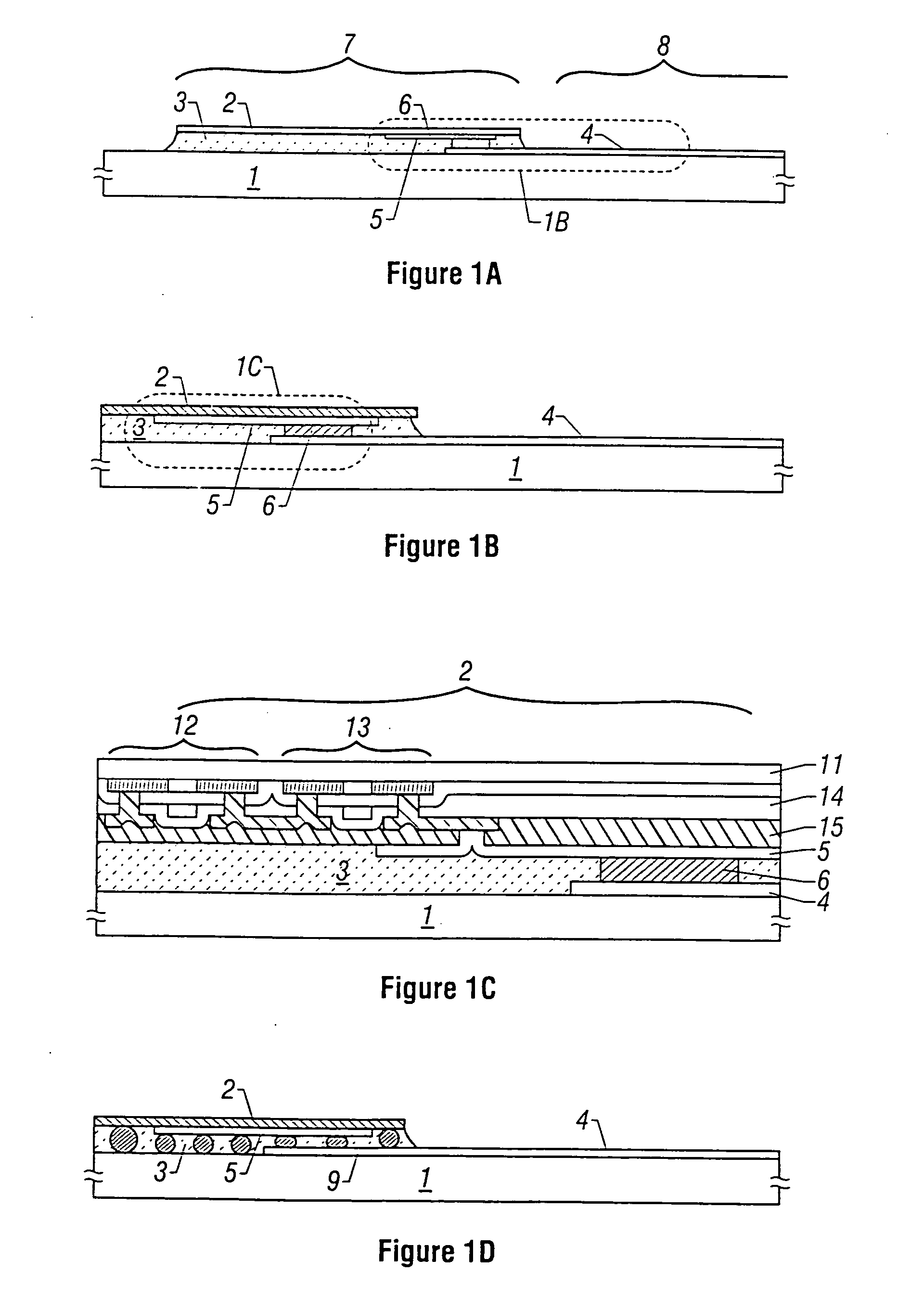
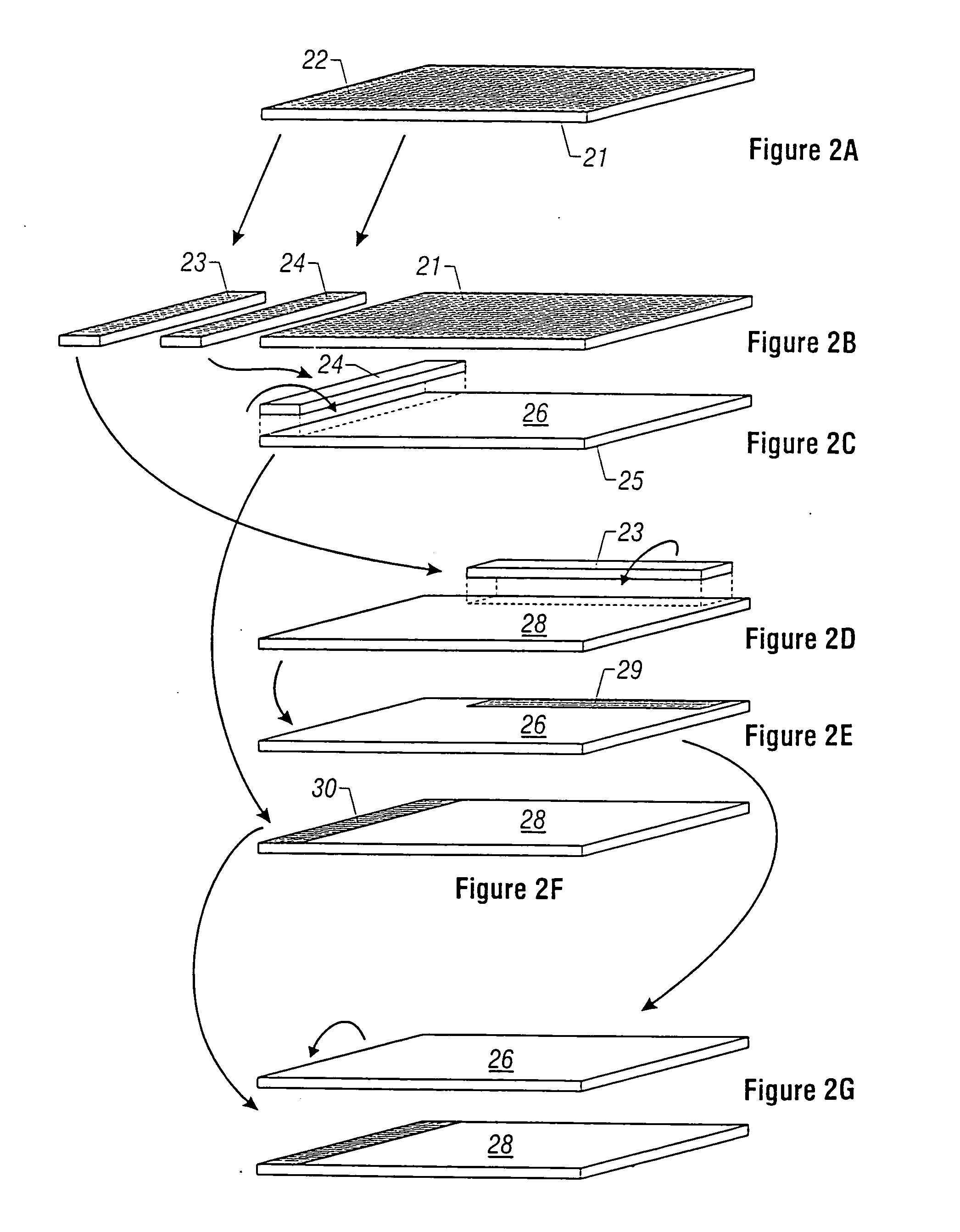
[0045] Manufacturing steps for fabricating one substrate of a passive matrix liquid crystal display are briefly described now. The present example is described by referring to FIGS. 4(A)-4(C) and 5(A)-5(D). Steps for forming a driver circuit on a stick crystal are schematically shown in FIGS. 4(A)-4(C). Steps for mounting the stick crystal on the substrate of the liquid crystal display are schematically shown in FIGS. 5(A)-5(D).

[0046] First, a silicon film having a thickness of 3000 Å was deposited as a peeling layer 32 on a glass substrate 31. Since the silicon film becoming the peeling layer 32 is etched away when circuitry and a substrate formed on the silicon film are separated, the quality of the silicon film will present almost no problems. Therefore, the silicon film may be deposited by a method which permits mass production. Furthermore, the silicon film may be either amorphous or crystalline in character.

[0047] The glass substrate may be made of Corning 7059 glass, Cornin...

example 2

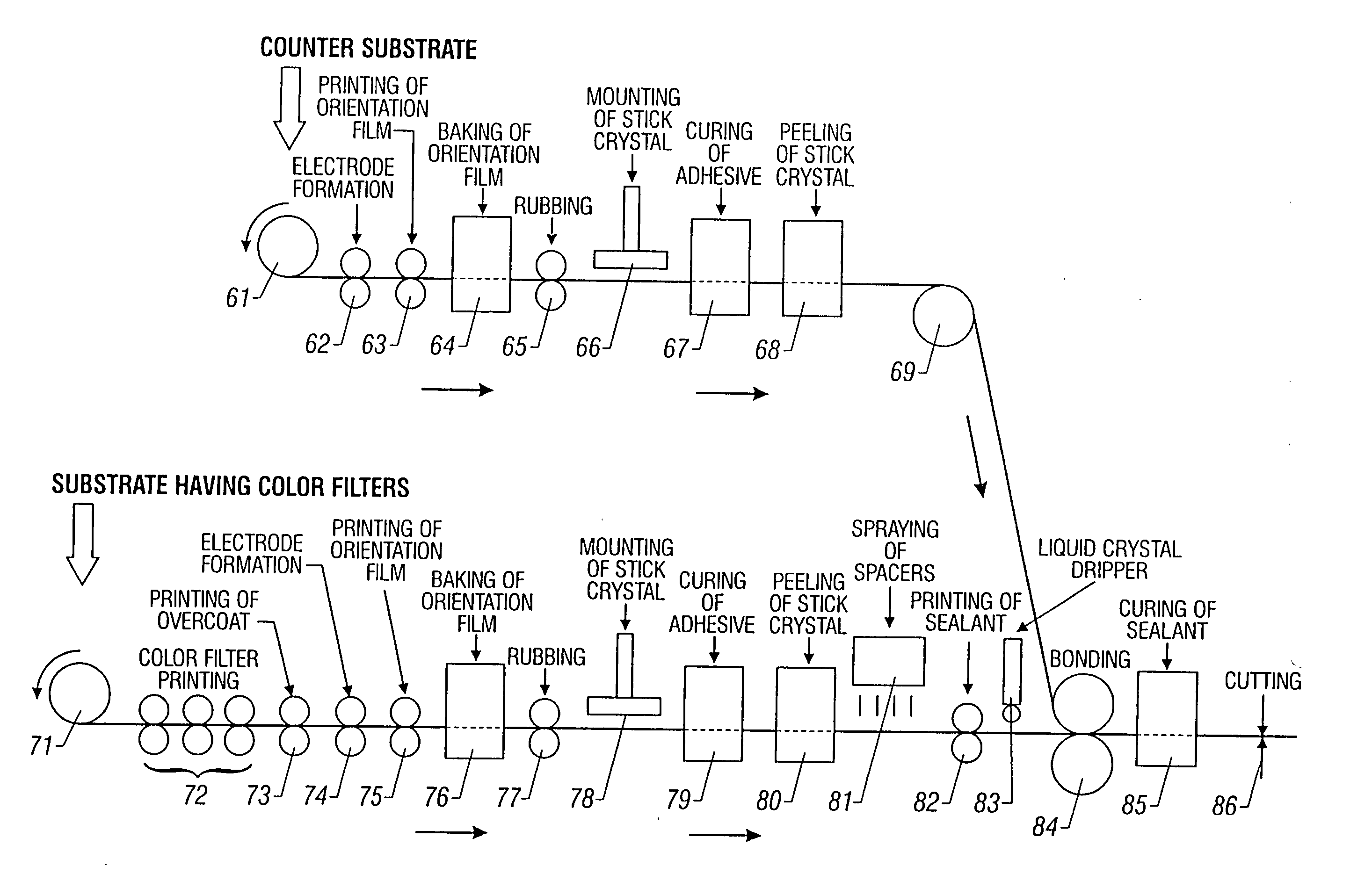
[0060] The present example relates to a method (referred to as the roll-to-roll method) of successively fabricating filmy passive matrix liquid crystal displays. A production system for implementing the present example is shown in FIG. 6. The substrate material for obtaining the filmy liquid crystal displays may be selected from polyethylene sulfite, poly-carbonate, and polyimide. Since polyethylene terephthalate and polyethylene naphthalate are polycrystalline plastics, they are not appropriate as liquid crystal materials which provide displays making use of polarization of light.

[0061] The production system shown in FIG. 6 is divided into two major parts: the upper portion and the lower portion. In the lower portion, a substrate on which color filters are formed is fabricated as a component of a liquid crystal display. In the upper portion, a counter substrate is manufactured. First, steps for fabricating the substrate on which the color filters are formed are described.

[0062] C...


PUM

PropertyMeasurementUnit
widthaaaaaaaaaa
thicknessaaaaaaaaaa
thicknessaaaaaaaaaa

Abstract

A method of fabricating a driver circuit for use with a passive matrix or active matrix electrooptical display device such as a liquid crystal display. The driver circuit occupies less space than heretofore. A circuit (stick crystal) having a length substantially equal to the length of one side of the matrix of the display device is used as the driver circuit. The circuit is bonded to one substrate of the display device, and then the terminals of the circuit are connected with the terminals of the display device. Subsequently, the substrate of the driver circuit is removed. This makes the configuration of the circuit much simpler than the configuration of the circuit heretofore required by the TAB method or COG method, because conducting lines are not laid in a complex manner. The driver circuit can be formed on a large-area substrate such as a glass substrate. The display device can be formed on a lightweight material having a high shock resistance such as a plastic substrate. Hence, a display device having excellent portability can be obtained.

Description

BACKGROUND OF THE INVENTION [0001] 1. Field of the Invention [0002] The present invention relates to a passive matrix or active matrix display such as a liquid crystal display and, more particularly, to a fashionable display device in which the ratio of the area of the display portion to the area of the substrates of the display device is increased by effectively mounting a driver semiconductor integrated circuit. [0003] 2. Description of the Related Art [0004] Passive matrix type and active matrix type constructions are known as matrix display devices. In the passive matrix type, a number of stripe-shaped conducting lines (row lines) made of a transparent conductive film or the like are arrayed in a certain direction on a first substrate. On a second substrate, similar stripe-shaped conducting lines (column lines) are arrayed in a direction substantially perpendicular to the conducting lines on the first substrate. Both substrates are so arranged that the conducting lines on them i...

Claims


Application Information

Patent Timeline
Patent Type & Authority Applications(United States)
IPC IPC(8): G02F1/13G02F1/1333G02F1/1343G02F1/1345G02F1/1362H01L21/00
CPCG02F1/1303G02F1/133305G02F1/1345G02F1/13452H01L2924/01079H01L21/67132H01L2221/68363H01L2224/16G02F1/13454
Inventor YAMAZAKI, SHUNPEITAKEMURA, YASUHIKONAKAJIMA, SETSUOARAI, YASUYUKI
Owner YAMAZAKI SHUNPEI
Why Eureka
Try Eureka