

Barrier polishing fluid
a technology of polishing fluid and barrier, which is applied in the direction of waterborne vessels, metal-working apparatus, constructions, etc., can solve the problems of affecting the transmission of electrical signals, affecting the removal of electrical signals, and dimensional defects in the circuit interconn
- Summary
- Abstract
- Description
- Claims
- Application Information
AI Technical Summary
Benefits of technology
Problems solved by technology
Method used
Image


Examples
example 1
Imine Derivatives as Polishing Agents for CMP
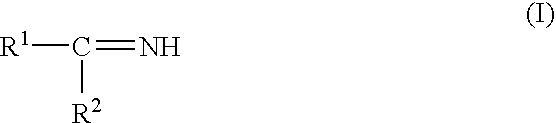
The imine derivative compounds listed in Table 1 were used as nitrogen-containing polishing agents for CMP. The structures listed under the headings “R1” and “R2 correspond to the substituents in structure (I):
TABLE 1Imine Derivative Compounds in Abrasive-Free Polishing FluidsTaNTEOSCuTestAdditiveR1R2Wt. %Å / minÅ / minÅ / min11,3-Diphenyl—NH—C6H5—NH—C6H522385−3110guanidine2Guanidine—NH2—NH2 {•HCl}21392−197hydrochloride3Tetramethyl-—N(CH3)2—N(CH3)221199127guanidine4Formamidine—H—NH222197−599acetate{•CH3COOH}5Acetamidine—CH3—NH2 {•HCl}1477180hydrochloride6Acetamidine—CH3—NH2 {•HCl}2450381hydrochlorideAo-Methylisourea—OCH3—NH22−8−226sulfate{•0.5 H2SO4}B1-Methyl-3-—NH—CH3—NH—NO22−18051nitroguanidineCArginine—NH2—NH—(CH2)3—2−18−519CH(NH2)—C(═O)OHDFormamidine-—NH2—S(═O)OH2139−175sulfinic acidEFormamidine-—NH2—S(═O)OH1−6285sulfinic acidF*2,2-Azobis—NH2—R21—N═N—R22—2−1−175(dimethyl-{•HCl}C(NH2)═NHpropionamidine)d{•HCl}i-HClG(control)———−15030
*R21 ...
example 2
Hydrazine Derivatives as Polishing Agents for CMP
The hydrazine derivative compounds listed in Table 2 were used as nitrogen-containing polishing agents for CMP. The results of the polishing are given in Table 3. The structures listed under the headings “R3” through “R6” correspond to the substituents in structure (II):
R3R4N—N R5R6 (II).
TABLE 2Hydrazine Derivative Compounds inAbrasive-Free Polishing FluidsAdditiveR3R4R5R6Carbohydrazide—H—H—H—C(═O)—NH—NH2Acetic hydrazide—H—H—H—C(═O)—CH3Semicarbazide—H—H—H—C(═O)—NH2hydrochloride{•HCl}Formic hydrazide—H—H—H—C(═O)H1,2-—H—C(═O)H—H—C(═O)HDiformylhydrazineMethylhydrazino-—H—CH3—H—C(═O)OHcarboxylateOxalic dihydrazide—H—H—H—(C(═O))2—NH—NH2Acetone azine—═C(CH3)2—═C(CH3)2
TABLE 3Hydrazine Derivative Compounds inAbrasive-Free Polishing FluidsWt. TaNTEOSCuTestAdditive%Å / minÅ / minÅ / min 8Carbohydrazide21435−274 9Carbohydrazide21059−37510Carbohydrazide21127−410111Carbohydrazide210841−3512Acetic hydrazide216031.413913Semicarbazide hydrochloride21...
PUM
| Property | Measurement | Unit |
|---|---|---|
| Percent by mass | aaaaa | aaaaa |
| Percent by mass | aaaaa | aaaaa |
| Fraction | aaaaa | aaaaa |
Abstract
Description
Claims
Application Information