Non-volatile memory device

a memory device and non-volatile technology, applied in nanoinformatics, instruments, transistors, etc., can solve problems such as affecting the threshold voltage of transistors, and achieve the effects of improving device retention characteristics, low cost, and tuning the conductivity of active layers

Active Publication Date: 2005-04-07
MASSACHUSETTS INST OF TECH
View PDF36 Cites 156 Cited by
  • Summary
  • Abstract
  • Description
  • Claims
  • Application Information

AI Technical Summary

Benefits of technology

Within the device, the nanoparticle can form a layer, for example a monolayer, on a substrate. The monolayer can be formed by methods or modification of methods described in U.S. application Ser. No. 10 / 400,907, filed Mar. 28, 2003, which is incorporated by reference in its entirety. The memory device can include a floating-gate field effect transistor. The core can be a semiconductor material, for example, a binary or ternary semiconductor material. The outer layer of each nanoparticle can electrically isolate each core, limiting or reducing lateral conduction in the layer. This structure can produce a non-volatile memory device that has program / erase characteristics comparable to conventional stacked gate non-volatile memory devices, excellent read / erase cycling performance, and improved long-term non-volatility in comparison to a thin, lower gate or, tunnel oxide-based memory device. The nanoparticle can include an overcoating between the core and the outer layer. The overcoating can be a semiconductor material.
The memory device can be a simple, low cost device fabrication since the organic layer and active layer can be prepared in a single step. The conductivity of the active layer can be tuned, which can improve the retention characteristics of the device. The structure of the device can enable the use of thinner structures.

Problems solved by technology

Injecting charge into the material can lead to tunneling from the channel, which can alter the threshold voltage of the transistor.

Method used


Image

  • Non-volatile memory device
  • Non-volatile memory device
  • Non-volatile memory device

Examples


Embodiment Construction

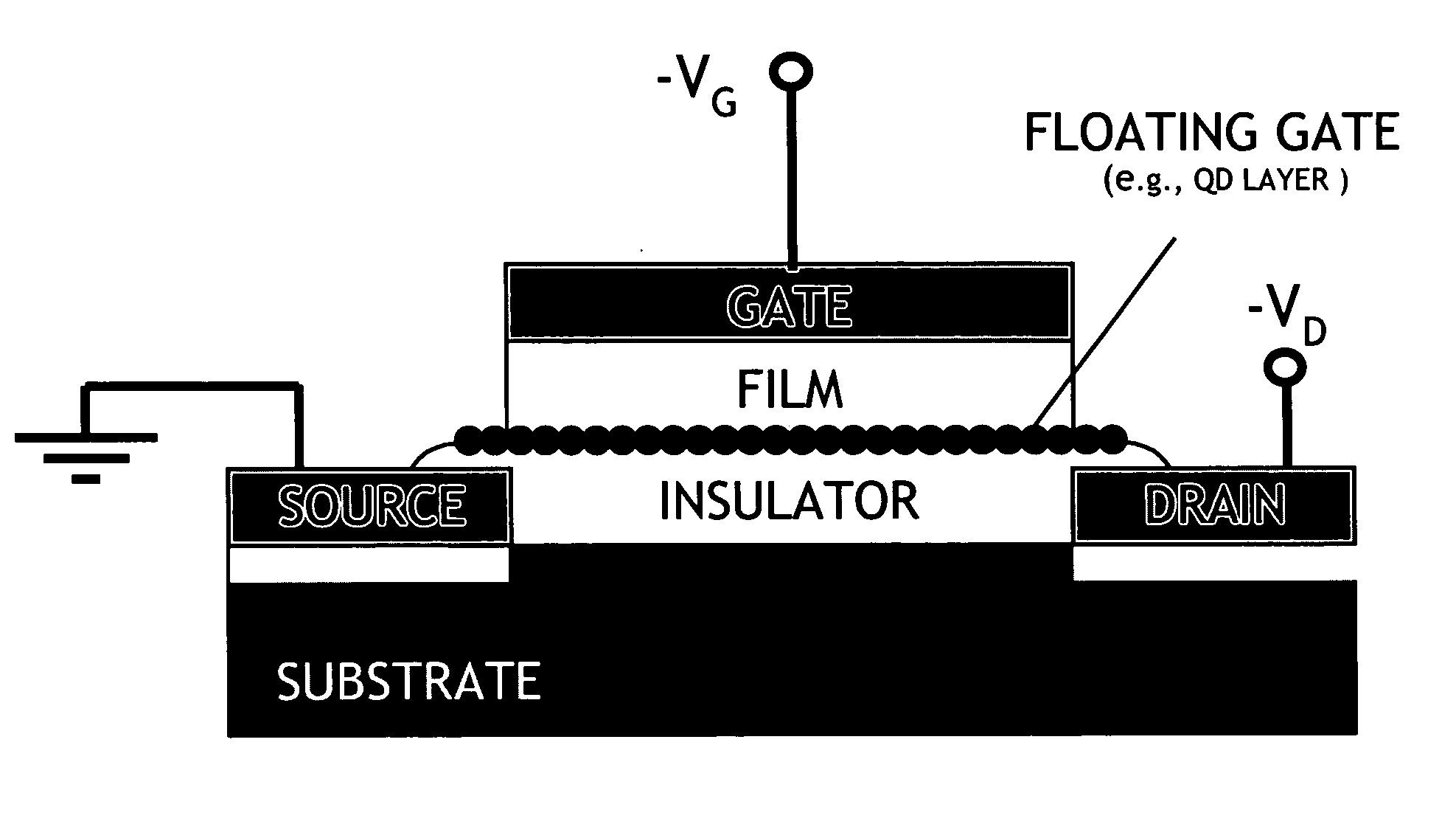
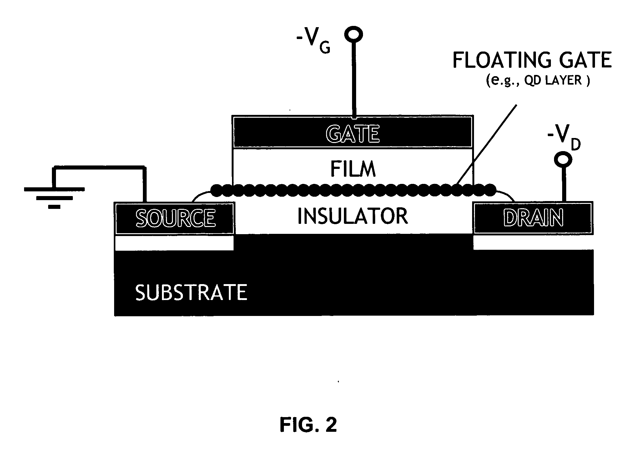
A memory device can include a room-temperature-integratable memory element. The memory element can be used in numerous electronic technology platforms, including organic, III-V, and even silicon electronics. The memory element can be a non-volatile memory device including a layer of charge trapping material having a selectable lateral conductivity, such as nanoparticles having a selectable outer layer. The memory element can be manufactured using room-temperature methodology to form a hybrid organic / inorganic device.

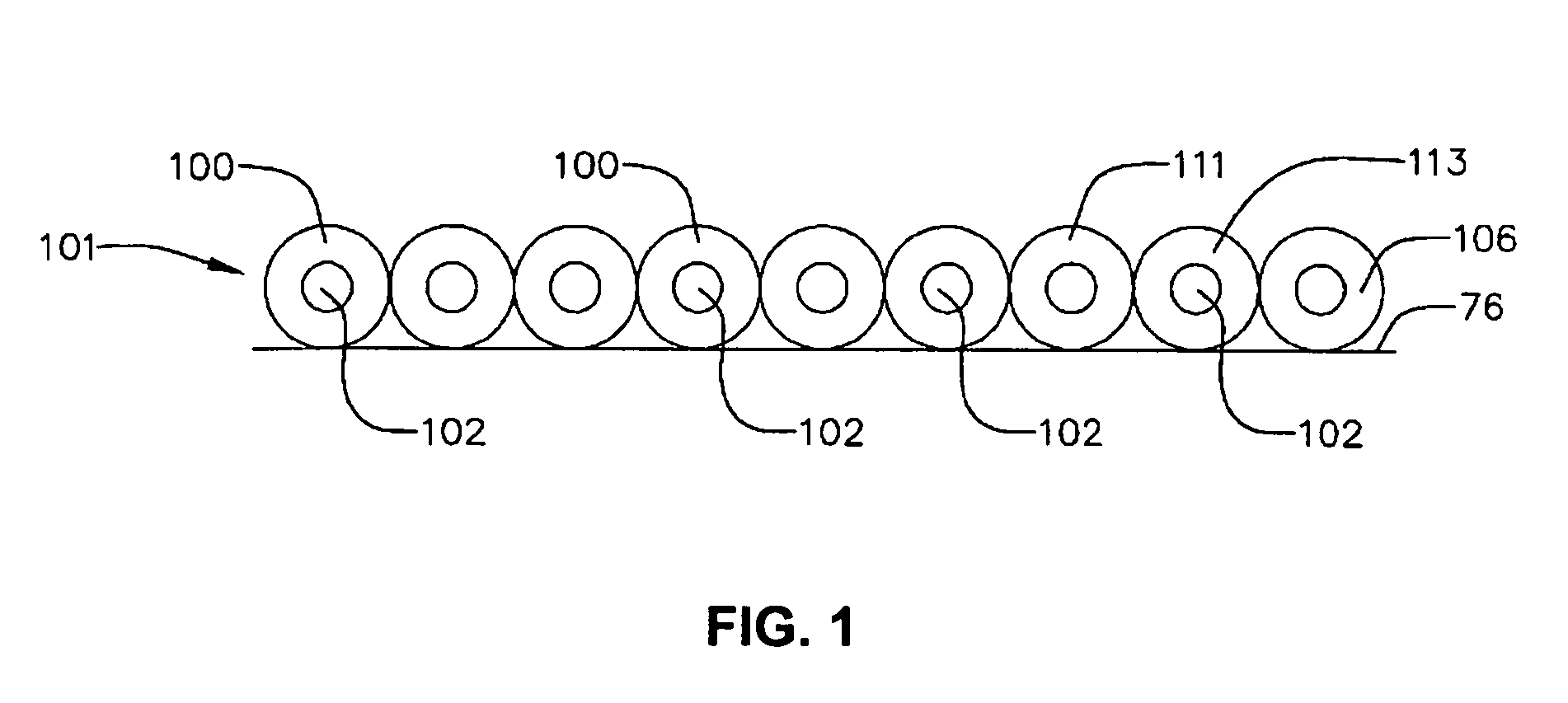
The memory element can be a chip-scale memory cell array. A chip-scale memory cell array can be formed by employing the charge trapping properties of nanoparticles monolayers. The individual memory cell configuration includes a field effect transistor structure in which nanoparticles form a floating gate. An example of this structure is shown in FIG. 1. The device is similar to other devices based on other materials, but has a number of advantages over those devices. Ex...


PUM


Abstract

A memory device can include an active layer that has a selectable lateral conductivity. The layer can include a plurality of nanoparticles.

Description

TECHNICAL FIELD The invention relates to a non-volatile memory device. BACKGROUND Non-volatile memory is a component of a growing number of portable products. Non-volatile floating gate memory devices can include a gate of metal-oxide semiconductor field effect transistors (MOSFETs). The memory operation of field effect transistors depends on charge storage of the material used to form the active portion of the device. In these floating gate memory devices, the material of the active portion of the device acts as a charge storage element located within the gate oxide of a MOSFET. Injecting charge into the material can lead to tunneling from the channel, which can alter the threshold voltage of the transistor. A typical write / read / erase cycle includes information being written by injecting charge from the channel into the material, reading by measuring the subthreshold current-voltage characteristics, and erasing by removing charge from the particles to the channel. The performance...

Claims


Application Information

Patent Timeline
Patent Type & Authority Applications(United States)
IPC IPC(8): G11C13/02G11C16/04H01LH01L21/28H01L29/423H01L29/788H01L31/0336
CPCB82Y10/00B82Y30/00G11C13/02G11C16/0466G11C2213/12G11C2213/18H01L29/7881G11C2216/06H01L21/28273H01L29/127H01L29/2203H01L29/42332G11C2213/53H01L29/40114
Inventor BAWENDI, MOUNGI G.BULOVIC, VLADIMIRCOE-SULLIVAN, SETH A.
Owner MASSACHUSETTS INST OF TECH
Why Eureka
Try Eureka