Direct digital amplitude modulator
a digital amplitude and modulator technology, applied in the direction of modulation, modulated carrier system, transmission, etc., can solve the problems of low power efficiency and insufficient linearity, difficult to filter out the alias signals of the dac output, and distortion of the desired signal, etc., to achieve easy integration, good linearity, and simple structure
- Summary
- Abstract
- Description
- Claims
- Application Information
AI Technical Summary
Benefits of technology
Problems solved by technology
Method used
Image
Examples
first embodiment
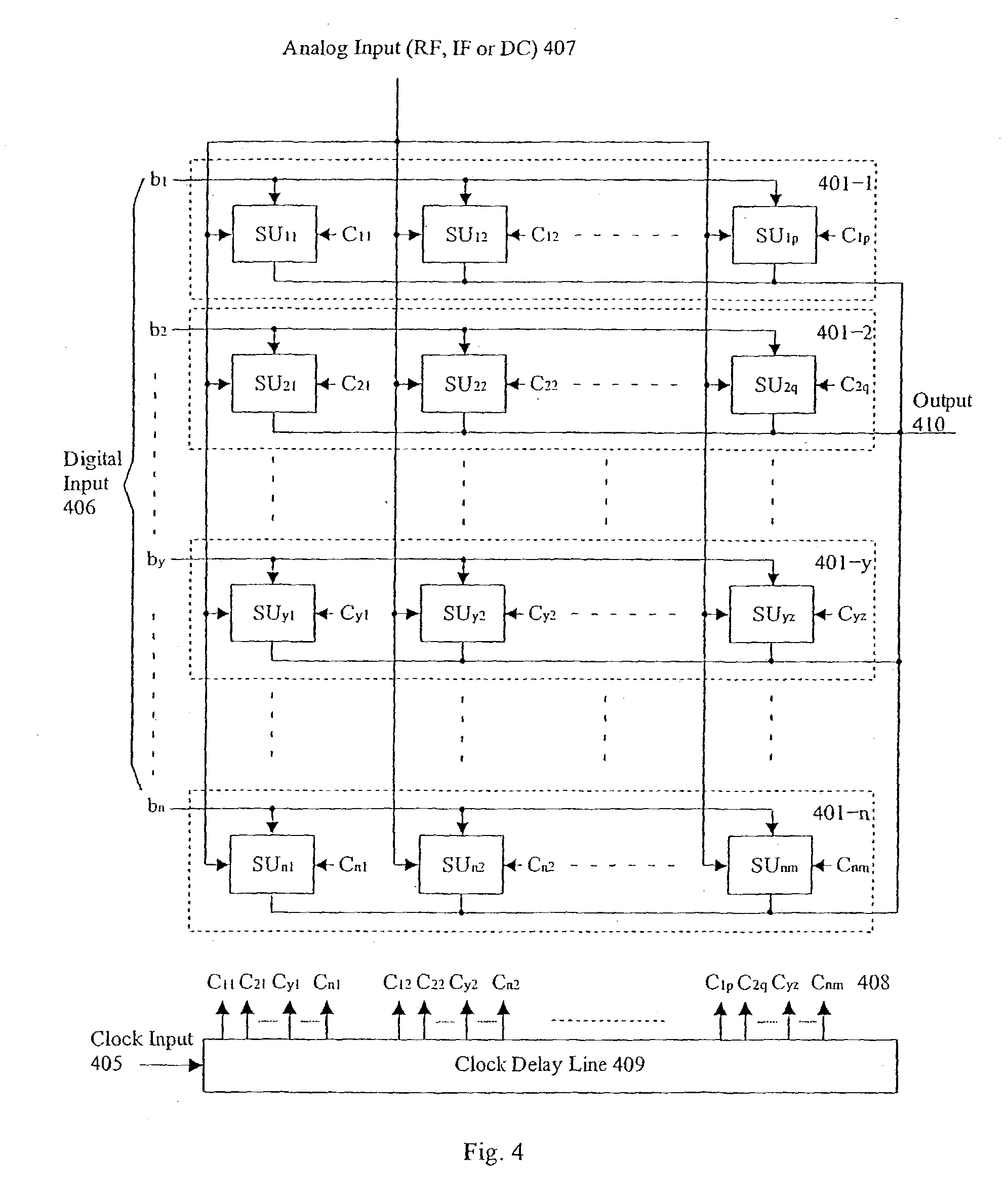
[0022]FIG. 5a shows the sub-switched current source units when the analog input is an RF or IF signal. Data signal 501 is obtained from DDAM's digital input signal 406, and clock signal 502 is obtained from clock delay line 409 in the DDAM. Data and clock signals 501 and 502 are sent to register 512 to produce output signal 503a and inverse output signal 503b. Transistors M4 510 and M5 511, controlled by output signal 503a and inverse output signal 503b of register 512 respectively, act as switches to current source transistor M3 509. The dimensions of transistors M4 510 and M5 511 can be properly selected in order to set the switching time constant together with the parasitic capacitance to obtain a hold character somewhere between zero-order-hold and first-order-hold. The RC charge and discharge hold (RCH) character can achieve higher attenuation for the alias signals. The differential RF or IF signals are fed to transistors M1 508a and M2 508b. The power supply is provided via tw...
second embodiment
[0024]FIG. 6 shows the sub-switched current source units when the analog input is a DC signal (i.e. the DC power supply). Data signal 601 is obtained from DDAM's digital input 406, and clock signal 602 is obtained from clock delay line 409 in the DDAM. They are sent to register 603. Output 604a and inverse output 604b of register 603 are sent to two switching transistors M1 607a and M2 607b. Bias signal 605 controls the bias of current source transistor M3 606. Load1 608a and Load2 608b (not include in each sub-switched current source unit) connected to power supply 610 are the loads of switching transistors M1 607a and M2 607b respectively, which can be active or passive, on-chip or off-chip. Differential baseband outputs 609a and 609b are obtained from the drains of switching transistors M1 607a and M2 607b, and either of them can be a single-ended output.
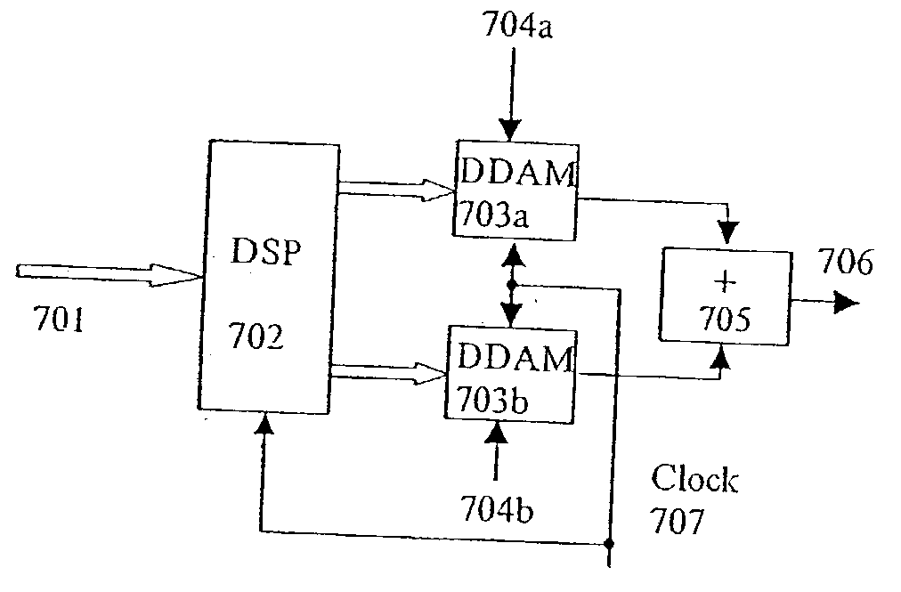
[0025]FIG. 7 shows a quadrature modulator for RF or IF carrier signal based on this invention. Data 701 to be transmitted is sp...
PUM
 Abstract
Description
Claims
Application Information


