
Reduced voltage pre-charge multiplexer

a voltage pre-charge and multiplexer technology, applied in the field of reducing the voltage pre-charge multiplexer, can solve the problems of select-to-output delay, different type of delay, low speed of prior art multiplexers, etc., and achieve low input to output delay, reduce path delay through a large multiplexer, and reduce the delay effect of input to outpu

Active Publication Date: 2005-04-14
ATMEL CORP
View PDF4 Cites 2 Cited by
  • Summary
  • Abstract
  • Description
  • Claims
  • Application Information

AI Technical Summary

Benefits of technology

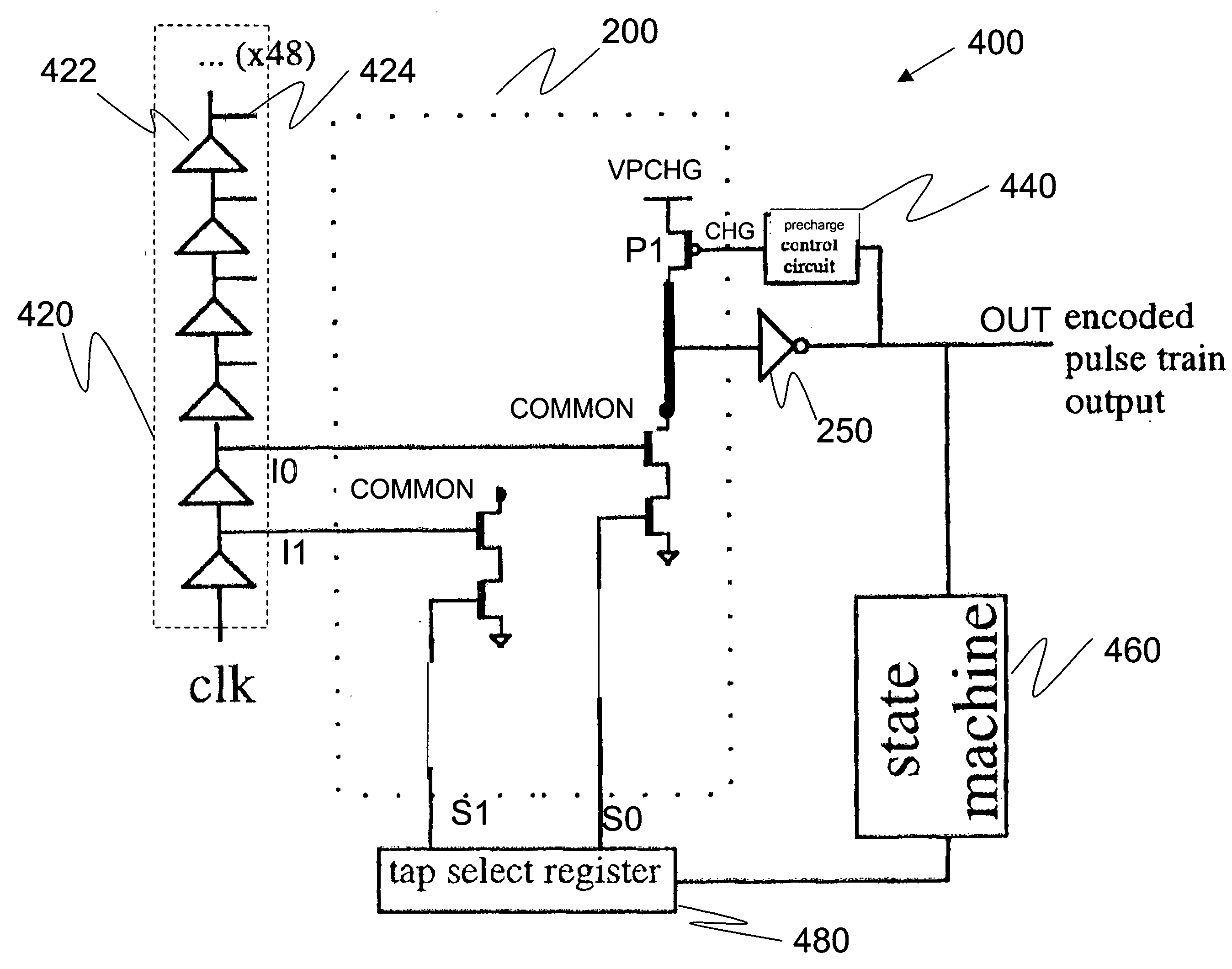
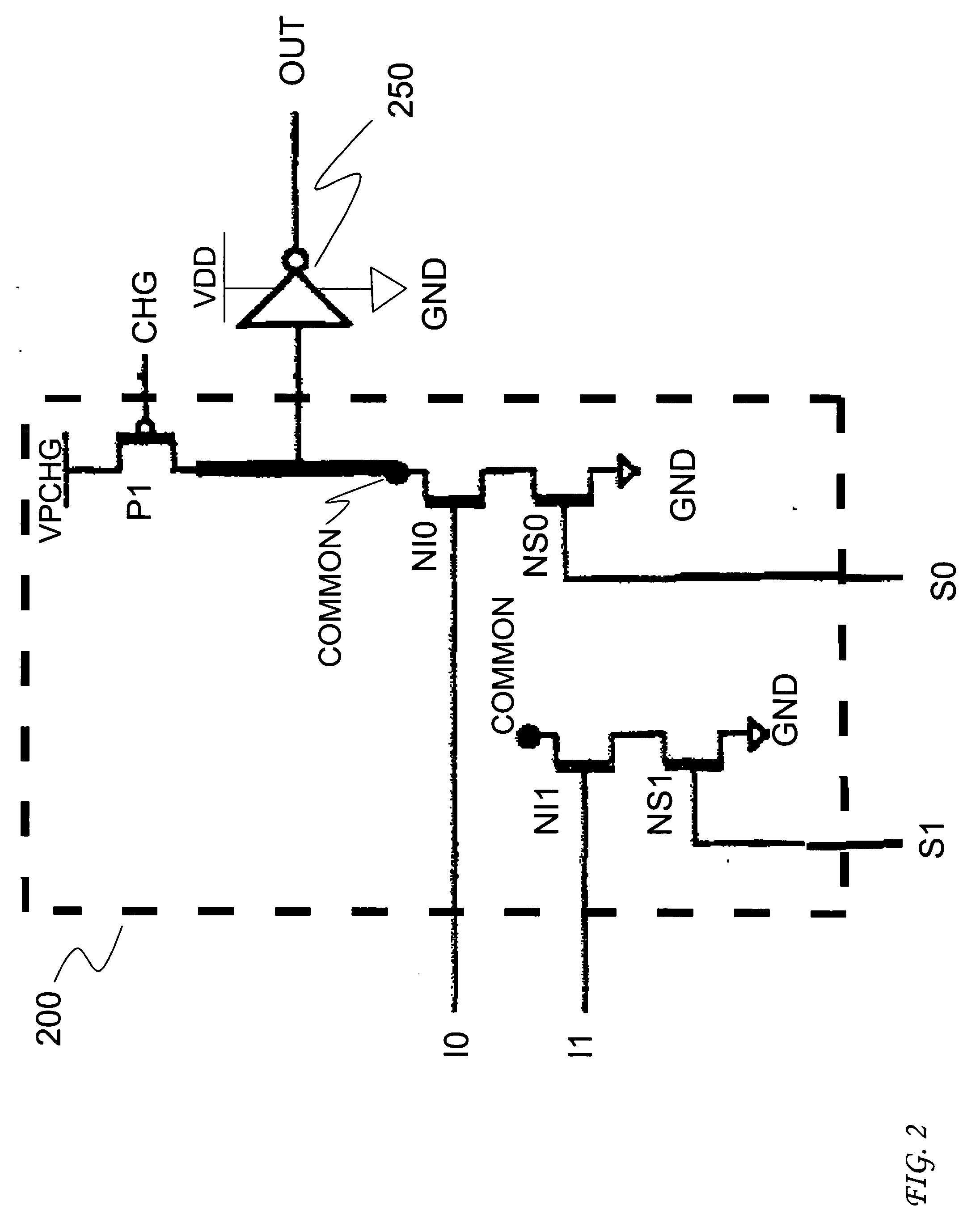
[0005] The present invention has a low input to output delay as well as a low select to output delay. The multiplexer is a common line with individual pulldowns for each input that are gated by selects. A reduced voltage pre-charge on the common line allows a quick response to a pulldown.
[0006] The reduced voltage pre-charge multiplexer of the present invention significantly reduces path delay through a large multiplexer. The multiplexer utilizes a common pre-charge node with input and select gated discharge paths. A pre-charge level is lowered to less than full voltage to further reduce path delay. The lower pre-charge voltage significantly reduces a time required to cause the common node to reach a switching point of the buffered output of the multiplexer.
[0007] Additionally, the present invention has a reduced stage depth for a given path providing an increased operating speed using a pre-charge / discharge approach to increase the path speed by reducing the load on the common line. The reduced voltage pre-charge significantly increases the operating speed over the pre-charge / discharge approach over the prior art.

Problems solved by technology

Prior art multiplexers suffer from low speeds due to factors such as 1) heavy loading on a common node and 2) depth of stages in a path (“stage depth”).
Each of these two factors produces a different type of delay.
The heavy loading on a common node causes a select-to-output delay.
The stage depth causes an input-to-output delay.

Method used


Image

  • Reduced voltage pre-charge multiplexer
  • Reduced voltage pre-charge multiplexer
  • Reduced voltage pre-charge multiplexer

Examples


Embodiment Construction

[0013] With reference to FIG. 2, an exemplary embodiment of a low pre-charge voltage multiplexer 200 is comprised of a PMOS pre-charge transistor P1, a first NMOS input transistor NI0, a first NMOS select transistor NS0, a second NMOS input transistor NS1, and a second NMOS select transistor NS1. An input signal I0 is coupled to the gate terminal of the first NMOS input transistor NI0. The drain terminal of the first input transistor NI0 is coupled to a common circuit node COMMON. The source terminal of the first NMOS input transistor NI0 is coupled to the drain terminal of the first NMOS select transistor NS0. A select signal S0 is coupled to the gate terminal of the first NMOS select transistor NS0. The source terminal of the first NMOS select transistor NS0 is coupled to a system ground potential GND. An input signal I1 is coupled to the gate terminal of the second NMOS input transistor NI1. The drain terminal of the second input transistor NI1 is coupled to the common circuit no...


PUM


Abstract

An electronic device selects one of a plurality of input signals for coupling to an output channel. Individual pulldowns provide a separate pathway for each input, and are coupled to a common node which is pre-charged to a voltage less than a system voltage. Each pulldown is coupled to a select line for gating an associated input signal.

Description

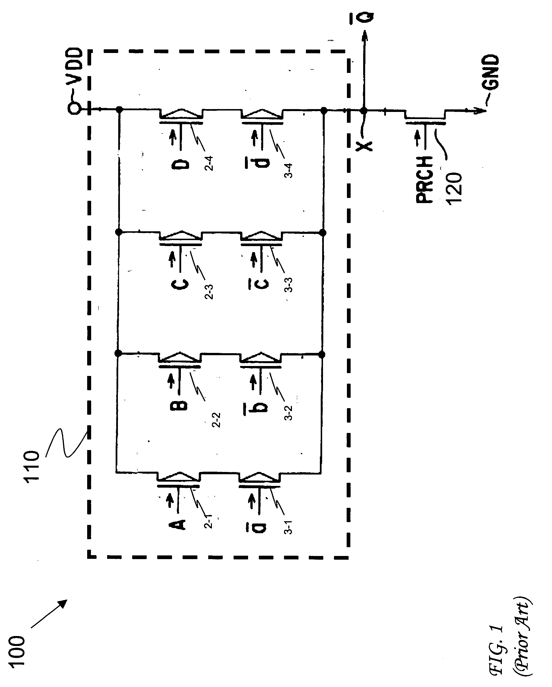
CROSS-REFERENCE TO RELATED APPLICATION [0001] This application claims priority from a U.S. Provisional Patent Application No. 60 / 510,710, filed Oct. 10, 2003.TECHNICAL FIELD [0002] The invention relates to a semiconductor integrated circuit device, and more particularly to a semiconductor integrated circuit device incorporating a multiplexer circuit utilizing a pre-charged node to increase signal throughput speed. BACKGROUND ART [0003] With respect to FIG. 1, a prior art multiplexer circuit 100, from U.S. Pat. No. 5,701,095 to Ohsawa, includes a data selecting circuit 110 and an NMOS pre-charge transistor 120. Input data signals A through D and selecting signals {overscore (a)} through {overscore (d)} (a-bar through d-bar) control the connection of a system supply potential VDD to a common node X providing an output signal {overscore (Q)} (Q-bar) by biasing the gate terminals of PMOS transistors 2-1 thru 2-4 and 3-1 thru 3-4. The common node X is charged to a system ground potential...

Claims


Application Information

Patent Timeline
Patent Type & Authority Applications(United States)
IPC IPC(8): H03K17/693
CPCH03K17/693
Inventor FAGAN, JOHN L.BOSSARD, MARK A.
Owner ATMEL CORP
Learn More