Method of controlling polysilicon crystallization

a technology of polysilicon and crystallization, which is applied in the direction of polycrystalline material growth, nuclear engineering, transportation and packaging, etc., can solve the problems of poor performance of polysilicon, worse than that of single crystalline silicon, and is not applicable to flat panel display fabrication. , to achieve the effect of improving the crystallization time, and improving the crystallization ra

Inactive Publication Date: 2005-04-14
IND TECH RES INST
View PDF4 Cites 23 Cited by
  • Summary
  • Abstract
  • Description
  • Claims
  • Application Information

AI Technical Summary

Benefits of technology

[0013] After dehydrogenation for the amorphous silicon layer, excimer laser annealing is performed, and the amorphous silicon layer is melted by absorbing laser energy. After cooling, the temperature of the melted silicon layer on the heat sink layer decreases more quickly than that in the opening. Nucleation sites are therefore formed in the melted silicon layer on the heat sink layer, and then lateral growth crystallization takes place towards the opening. Finally, polysilicon having grain size of micrometers with high grain order is obtained. Besides, an additional heating function by the heating layer helps to keep the laser energy transfer more uniform, and thus the crystallization time is lengthened to form larger and uniform lateral grains.
[0014] With the application of the polysilicon crystallization controlling method of the present invention, the polysilicon crystallization can be controlled well. In accordance with the present invention, thin film transistor devices can be further fabricated well by controlling crystal location.

Problems solved by technology

The electrical performance of polysilicon is better than that of amorphous silicon but worse than that of single crystalline silicon.
The conventional method for fabricating polysilicon film is solid phase crystallization (SPC), but SPC is not applicable to flat panel display fabrication because the upper-limit process temperature of a glass substrate is 650° C. Besides, the direct chemical vapor phase deposition (CVD) method is also used.
In SPC and CVD, the grain size of polysilicon is as small as 100 nm, and therefore the performance of polysilicon film is limited.
However, ELA is still not sufficient for future flat panel displays with high performance.
Besides, the grain size distribution is not uniform because of irregular laser energy deviation, and the electrical performance of devices, such as carrier mobility and uniformity of threshold voltage, is decreased.
The existence of grain boundaries leads to a rise in threshold voltage and leakage current, and a decrease in carrier mobility and device stability.

Method used


Image

  • Method of controlling polysilicon crystallization
  • Method of controlling polysilicon crystallization
  • Method of controlling polysilicon crystallization

Examples


embodiment 1

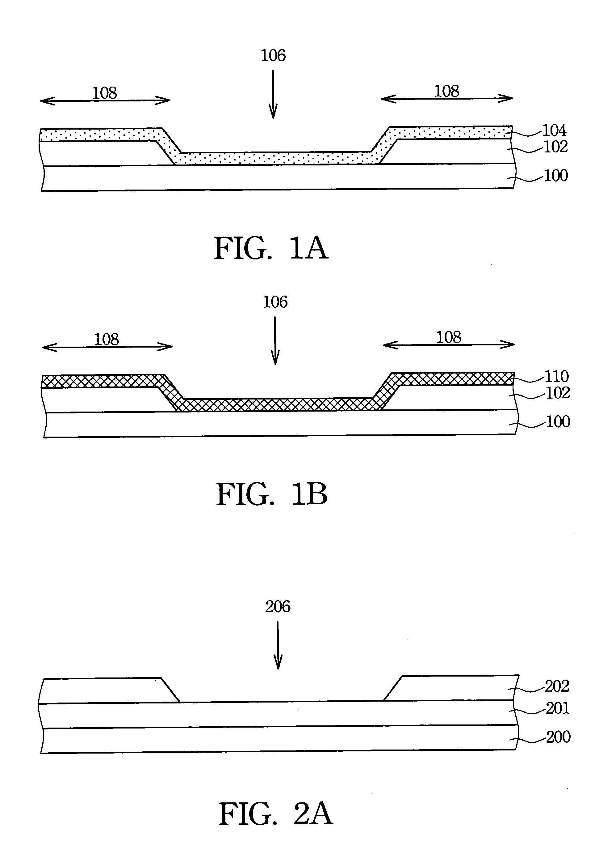
[0022] The present invention discloses a method of controlling polysilicon crystallization. Referring to FIG. 1A, a heat sink layer 102 with a high heat conductive coefficient is first formed on a substrate 100 by, for example, plasma enhanced chemical vapor phase deposition (PECVD). The substrate 100 may be a glass substrate for display fabrication, and the heat sink layer 102 is a high heat conductivity material such as silicon nitride (SiNx) with heat conductive coefficient of 16-33 W / m2k. The preferable thickness of the heat sink layer 102 is about 100 nm.

[0023] Then, the heat sink layer 102 is patterned by, for example, photolithography and etching to form an opening 106. The foregoing etching may be plasma dry etching performed by providing gases with carbon ionic molecules such as, for example, carbon tetrafluoride (CF4). Next, an amorphous silicon layer 104 is formed on the heat sink layer 102 and in the opening 106 by, for example, PECVD or physical vapor deposition (PVD),...

embodiment 2

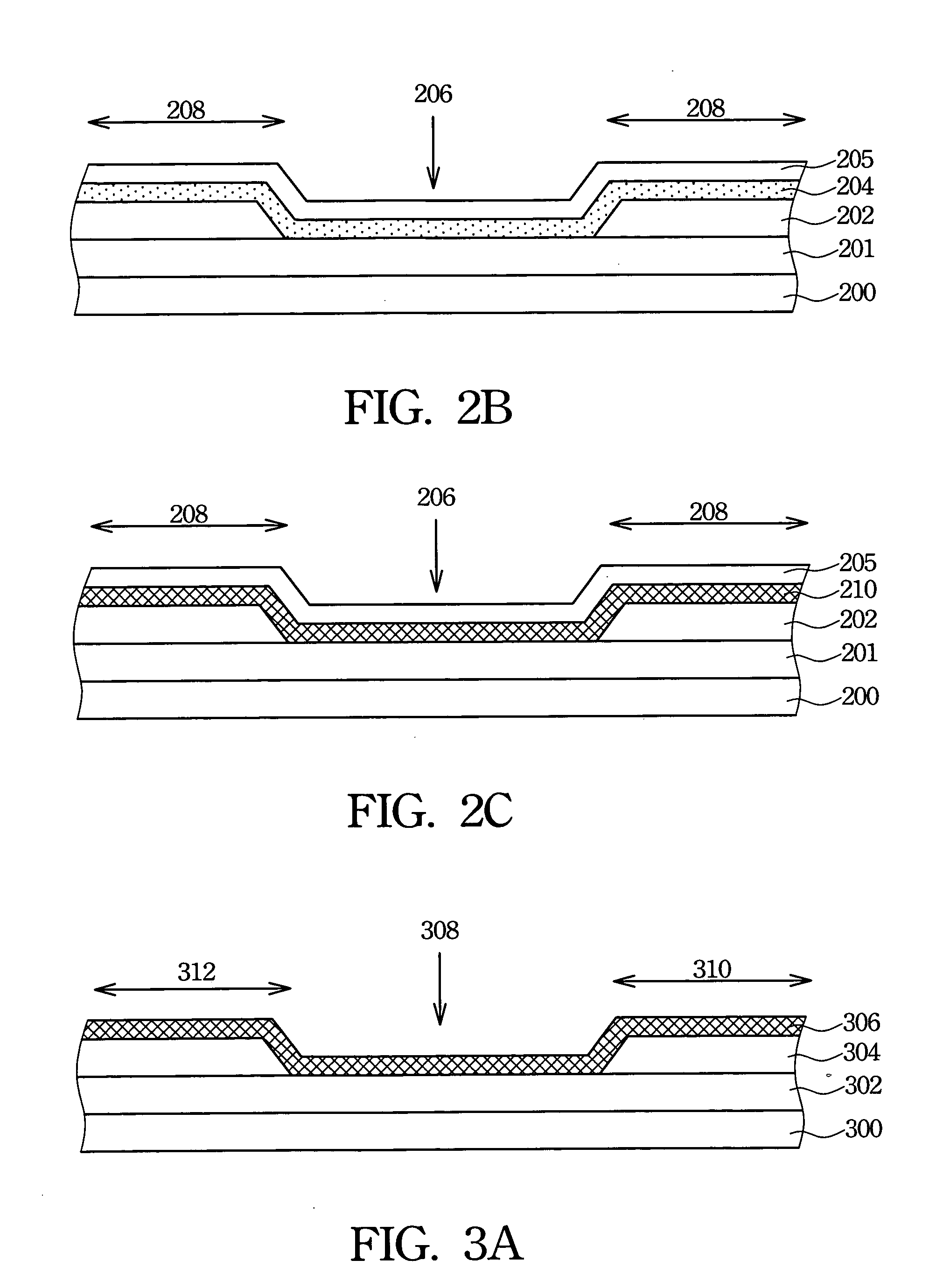
[0026] The present invention discloses another method of controlling polysilicon crystallization. In addition to a material having high heat transfer property being used a heat sink layer, a heating layer having a heating function and a heat resist layer that retains warmth are also added to form another films structure for controlling polysilicon crystallization.

[0027] Referring to FIG. 2A, a heat resist layer 201 with a low heat conductive coefficient is first formed on a substrate 200 by, for example, PECVD, PVD, spin coating or solution-gelation (Sol-Gel). The substrate 200 may be a glass substrate, and the heat resist layer 201 is a poor heat conductor such as silicon oxide (SiOx) with heat conductive coefficient of 1.4 W / m2k. The heat conductivity of the heat resist layer is less than that of the substrate. Then, a heat sink layer 202 with a high heat conductive coefficient is formed on the heat resist layer 201 by, for example, PECVD. The heat sink layer 202 is a good heat c...

embodiment 3

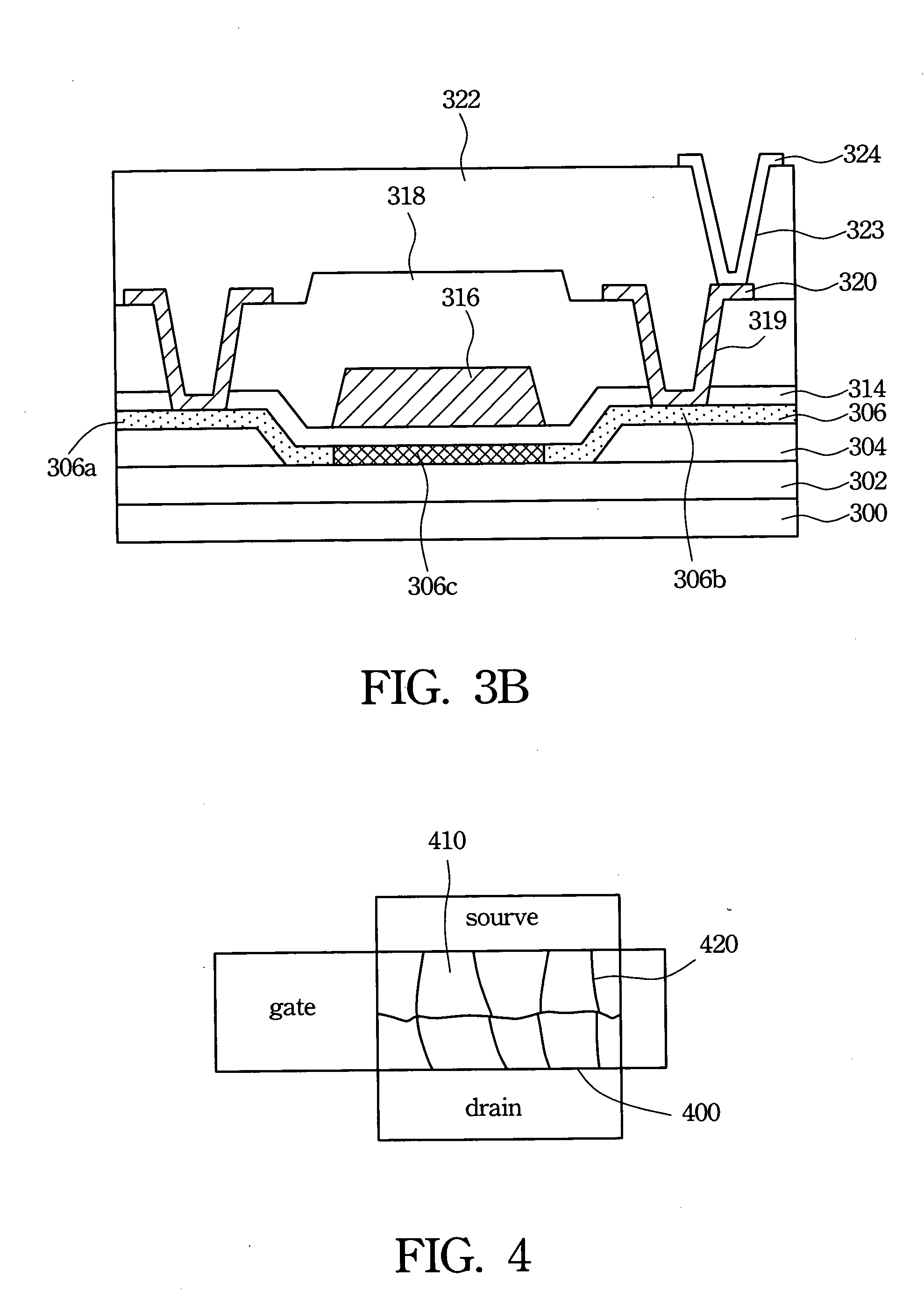
[0034] With the embodiments of the present invention employed, thin film materials chosen and structures designed, superior lateral growth polysilicon is obtained merely by excimer laser annealing; in addition to grain size, crystal location, grain order and uniformity of grain size are controlled well. Thus, the present invention can be further employed in thin film transistors fabrication to obtain devices with higher carrier mobility.

[0035]FIG. 3A illustrates a cross-sectional view of forming a channel region in a thin film transistor in accordance with a preferred embodiment of the present invention. When forming a thin film transistor structure of the present invention, a buffer layer 302 is first formed on a substrate 300 by, for example, PECVD. The substrate 300 may be a glass substrate, and materials of the buffer layer 302 may be SiOx. Then, a method of controlling polysilicon crystallization, for example, the first preferred embodiment of the present invention is used.

[0...


PUM

PropertyMeasurementUnit
grain sizeaaaaaaaaaa
thicknessaaaaaaaaaa

Abstract

A heat sink layer is formed on portions of a substrate, and then an amorphous silicon layer is formed thereon. The heat coefficient of the heat sink layer is greater than that of the substrate. When an excimer laser heats the amorphous silicon layer to crystallize the amorphous silicon, nucleation sites are formed in the amorphous silicon layer on the heat sink layer. Next, laterally expanding crystallization occurs in the amorphous silicon layer on the substrate to form polysilicon having a crystal size of a micrometer.

Description

FIELD OF THE INVENTION [0001] The present invention relates to a method of fabricating a polysilicon film of polysilicon thin film transistors, and more particularly, to a method of controlling polysilicon crystallization. BACKGROUND OF THE INVENTION [0002] There are many forms of the silicon material generally used in semiconductors, such as amorphous, polycrystalline and single crystalline silicon. Polycrystalline silicon (polysilicon) thin film has lately attracted considerable attention due to its special physical properties and low cost in thin film transistor (TFT) fabrication, especially in the application of thin film transistor liquid crystal displays (TFT-LCD). [0003] The electrical performance of polysilicon is better than that of amorphous silicon but worse than that of single crystalline silicon. Polysilicon is an aggregate of single crystal grains and thus there are many grain boundaries; so grain size enlargement and grain boundary reduction for polysilicon are very i...

Claims


Application Information

Patent Timeline
Patent Type & Authority Applications(United States)
IPC IPC(8): B05D5/12C30B13/24C30B29/06H01L21/20H01L21/336H01L21/77H01L29/04H01L29/786
CPCC30B13/24C30B29/06H01L21/2026H01L29/78603H01L27/1296H01L29/04H01L29/66757H01L27/1281H01L21/02686H01L21/02422H01L21/02488H01L21/02502H01L21/02532H01L21/02595
Inventor LIN, JIA-XINGCHEN, CHI-LINCHEN, YU-CHENGLUO, YIH-RONG
Owner IND TECH RES INST
Why Eureka
Try Eureka