Method of heat treatment, method for forming wiring pattern, method for manufacturing electro-optic device, and electro-optic device and electronic apparatus

a technology of wiring pattern and heat treatment method, which is applied in the direction of conductive pattern formation, light absorption dielectrics, dielectric characteristics, etc., can solve the problems of long time-consuming treatment, long time-consuming deformation of substrates, and preventing increase in productivity, so as to achieve short time, efficient conversion of thermal energy, and the effect of increasing productivity

Inactive Publication Date: 2005-04-14
SEIKO EPSON CORP
View PDF6 Cites 12 Cited by
  • Summary
  • Abstract
  • Description
  • Claims
  • Application Information

AI Technical Summary

Benefits of technology

[0007] In order to address or overcome the foregoing and / or disadvantages, a heat treatment method is provided in which an object is heat-treated with a light-to-heat converting material to convert light energy into thermal energy, by exposing a base material having the light-to-heat converting material to light with the base material opposed to the object. Since the base material includes the light-to-heat converting material, the light energy of emitted light can be effectively converted into thermal energy. Consequently, a sufficient amount of thermal energy is applied to the object to heat-treat it. The emitted light irradiates the light-to-heat converting material to increase temperature instantaneously. Accordingly, the object can be heat-treated in a short time. In addition, since the thermal energy is instantaneously applied to the object, the object (substrate) is not affected even if it contains a non-heat resistant material, such as plastic.
[0016] An electro-optic device of an exemplary aspect of the present invention includes a wiring pattern formed by the foregoing wiring pattern forming method. Another electro-optic device of an exemplary aspect of the present invention is manufactured by the method to manufacture an electro-optic device. An electronic apparatus of an exemplary aspect of the present invention includes the foregoing electro-optic device. According to an exemplary aspect of the present invention, electro-optic devices and electronic apparatus including the electro-optic devices can be manufactured with high productivity, and the resulting devices and apparatus can exhibit desired performance.

Problems solved by technology

Thus, the heat treatment takes a long time and prevents increase in productivity.
In addition, if a non-heat resistant material, such as plastic, is used in the substrate, heat treatment performed at high temperature for a long time deforms the substrate or causes other disadvantages.

Method used


Image

  • Method of heat treatment, method for forming wiring pattern, method for manufacturing electro-optic device, and electro-optic device and electronic apparatus
  • Method of heat treatment, method for forming wiring pattern, method for manufacturing electro-optic device, and electro-optic device and electronic apparatus
  • Method of heat treatment, method for forming wiring pattern, method for manufacturing electro-optic device, and electro-optic device and electronic apparatus

Examples


example

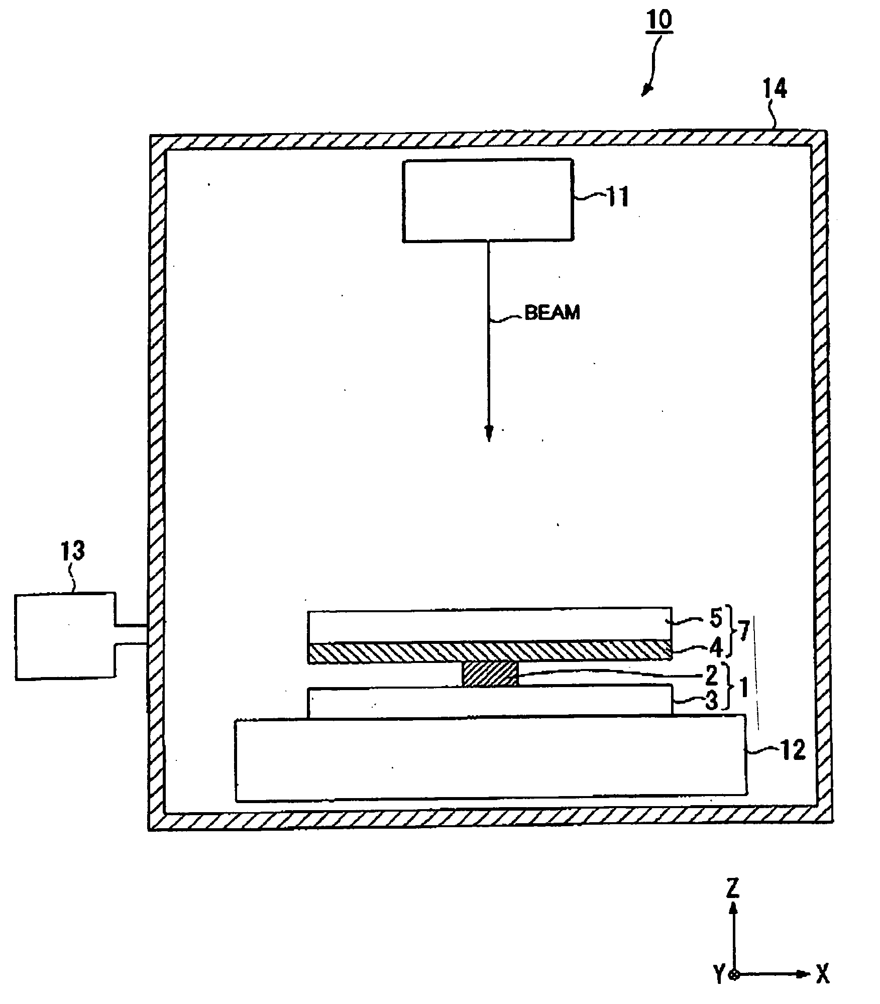
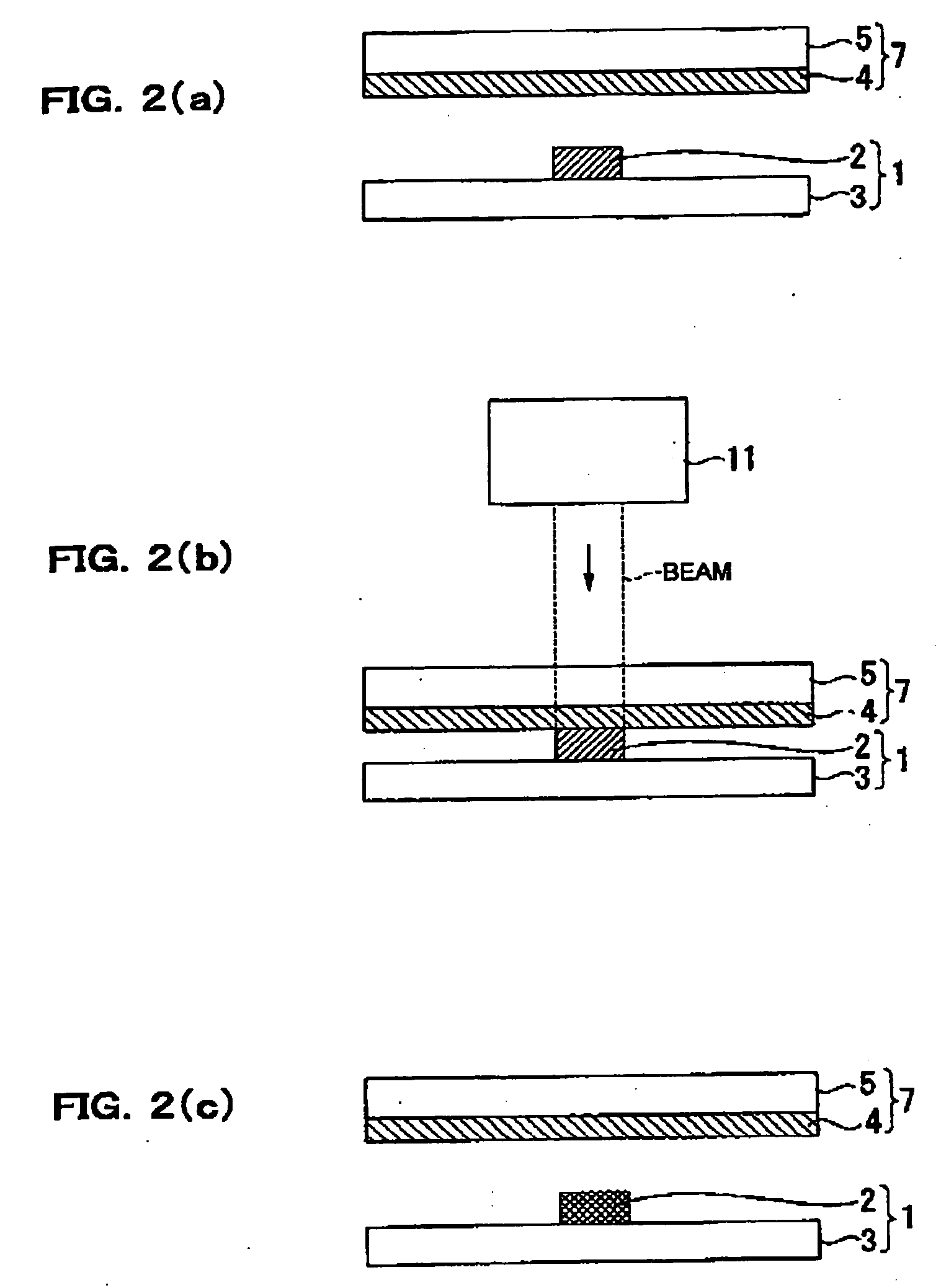
[0060] A polycarbonate sheet with a thickness of about 0.2 mm was used as the base material 5 of the heat treatment sheet 7. The sheet was coated with a thermosetting epoxy resin containing carbon black at a thickness of about 2 μm. The epoxy resin was cured into a light-to-heat conversion layer 4. A silver ink material layer was deposited on a poly(ethylene terephthalate) (PET) film to prepare an object 1 by a liquid discharge technique. The film or the object was held by a rotating drum in such a manner that the surface having the material layer faces outward, and the heat treatment sheet was wound over the film in such a manner that the surface having the light-to-heat conversion layer faces inward. Thus, the light-to-heat conversion layer was brought into close contact with the film. While the rotation drum was rotated at a speed of 50 rpm, a laser beam having a wavelength of 830 nm was emitted twice onto the sheet from a 14 W infrared semiconductor laser. The silver ink took on...


PUM

PropertyMeasurementUnit
temperaturesaaaaaaaaaa
wavelengthaaaaaaaaaa
thicknessaaaaaaaaaa

Abstract

To provide a heat treatment method to efficiently heat-treat an object without depending on the material of the object, a heat treatment layer includes a light-to-heat conversion layer to convert light energy into thermal energy and a base material. The heat treatment sheet is opposed to an object and exposed to light. Thus, the object is heat-treated by thermal energy generated from the light-to-heat conversion layer.

Description

BACKGROUND OF THE INVENTION [0001] 1. Field of Invention [0002] Exemplary aspects of the present invention relate to a method of heat treatment, a method to form a wiring pattern, a method to manufacture an electro-optic device, and an electro-optic device and an electronic apparatus. [0003] 2. Description of Related Art [0004] A related art conductive thin-film deposited on a substrate is often modified by heat treatment. Japanese Unexamined Patent Application Publication No. 5-21387 discloses a technique of laser annealing to modify a metallic thin film formed on a substrate by exposure to laser light. SUMMARY OF THE INVENTION [0005] A functional liquid containing a conductive material, applied onto a substrate is heat-treated (fired) to develop conductivity. However, such heat treatment must be performed at temperatures of at least 300° C. for 30 minutes or more. Thus, the heat treatment takes a long time and prevents increase in productivity. In addition, if a non-heat resistant...

Claims


Application Information

Patent Timeline
Patent Type & Authority Applications(United States)
IPC IPC(8): H01L21/288B32B3/26H01L21/268H01L21/3205H05B33/10H05B33/26H05K1/09H05K3/00H05K3/02H05K3/10H05K3/22
CPCH01L21/268H05K1/092H05K2203/1105H05K2201/0112H05K2203/107H05K3/22Y10T428/249953H05B33/10H05B33/26
Inventor TOYODA, NAOYUKI
Owner SEIKO EPSON CORP
Why Eureka
Try Eureka