Direct bumping on integrated circuit contacts enabled by metal-to-insulator adhesion

a technology of integrated circuit contacts and adhesion, which is applied in the direction of semiconductor devices, semiconductor/solid-state device details, electrical apparatus, etc., can solve the problems of brittleness, mechanical weakening of materials, and sensitivity to thermo-mechanical stress, so as to facilitate the rerouting of solder bumps, improve the adhesion of under-bump metal layers, and prevent stress-related damage to brittleness

Inactive Publication Date: 2005-04-21
TEXAS INSTR INC
View PDF1 Cites 43 Cited by
  • Summary
  • Abstract
  • Description
  • Claims
  • Application Information

AI Technical Summary

Benefits of technology

[0009] In another embodiment, the buffer metal layer is remote from the window to the IC metallization, but connected to the window by a rerouting trace of the seed metal. By rerouting, the reflow bumps may be positioned in a more uniform, less crowded pattern, and may also permit larger reflow bump sizes. Further, at the remote bump positions, thicker buffer layers are available to mitigate thermo-mechanical stresses and thus protect neighboring brittle low-k dielectrics materials.
[0013] Embodiments of the present invention are related to solder-ball and wire-bonded IC assemblies, semiconductor device packages, surface mount and chip-scale packages. It is a technical advantage that the invention offers a low-cost method of improving the adhesion of under bump metal layers to insulating layers, especially polymer insulators. It is an additional technical advantage that the invention facilitates the rerouting of solder bump and wire bond locations to contact pads, thus offering a method to distribute the interconnecting reflow bumps more uniformly over the whole device area and to prevent stress-related damage to brittle low-k dielectric layers under the contact pads. Further technical advantages include the opportunity to scale the assembly to smaller dimensions, supporting the ongoing trend of IC miniaturization, and to distribute the chip contacts more evenly over the chip area rather than restricting the contacts to a linear arrangement along the chip perimeters.

Problems solved by technology

However, changes implemented in the chip structure to satisfy the ongoing trends of device miniaturization and higher circuit speeds have recently confronted the flip-chip assembly technology with several new challenges.
This process, though, has a number of drawbacks due to technical and cost issues.
These materials are mechanically much weaker than the conventional silicon dioxide layers, and therefore much more sensitive to thermo-mechanical stress.
These stresses tend to fatigue the joints and the bumps, and result in cracks in solder joints and underlying insulating chip materials, resulting in eventual failure of the assembly.
The polymer has to be heat tolerant enough to withstand the solder reflow temperature, but it is poorly suited for adhesion to the under bump metals.

Method used


Image

  • Direct bumping on integrated circuit contacts enabled by metal-to-insulator adhesion
  • Direct bumping on integrated circuit contacts enabled by metal-to-insulator adhesion
  • Direct bumping on integrated circuit contacts enabled by metal-to-insulator adhesion

Examples


Embodiment Construction

[0020] The present invention is related to U.S. patent application Ser. No. 10 / 086,117, filed on Feb. 26, 2002 (Bojkov et al., “Waferlevel Method for Direct Bumping on Copper Pads in Integrated Circuits”).

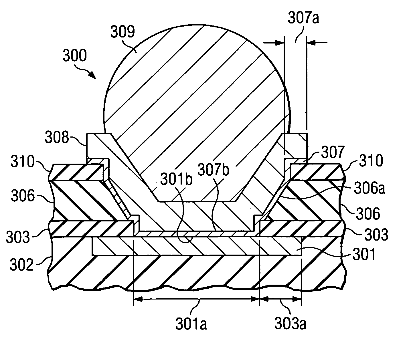
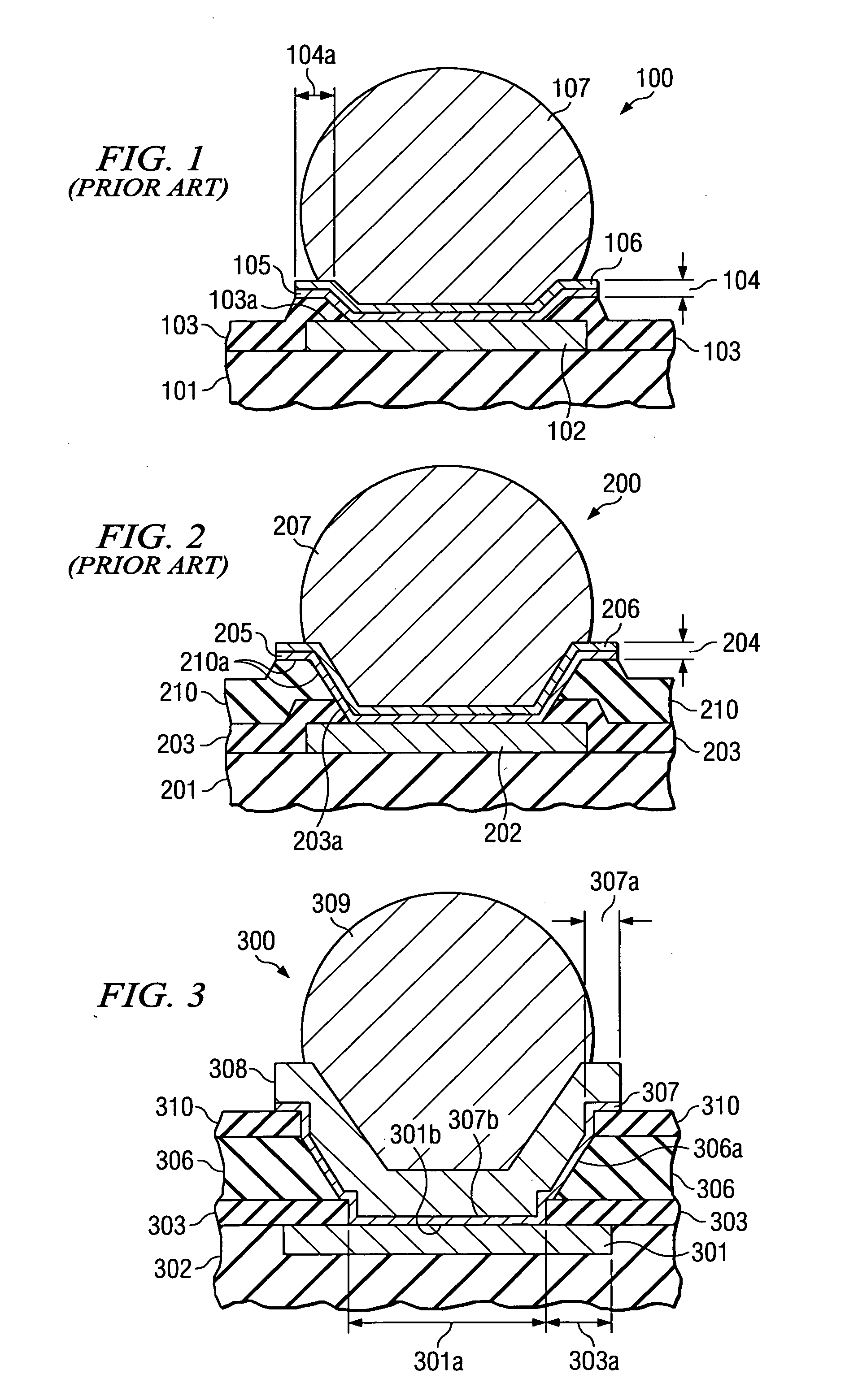
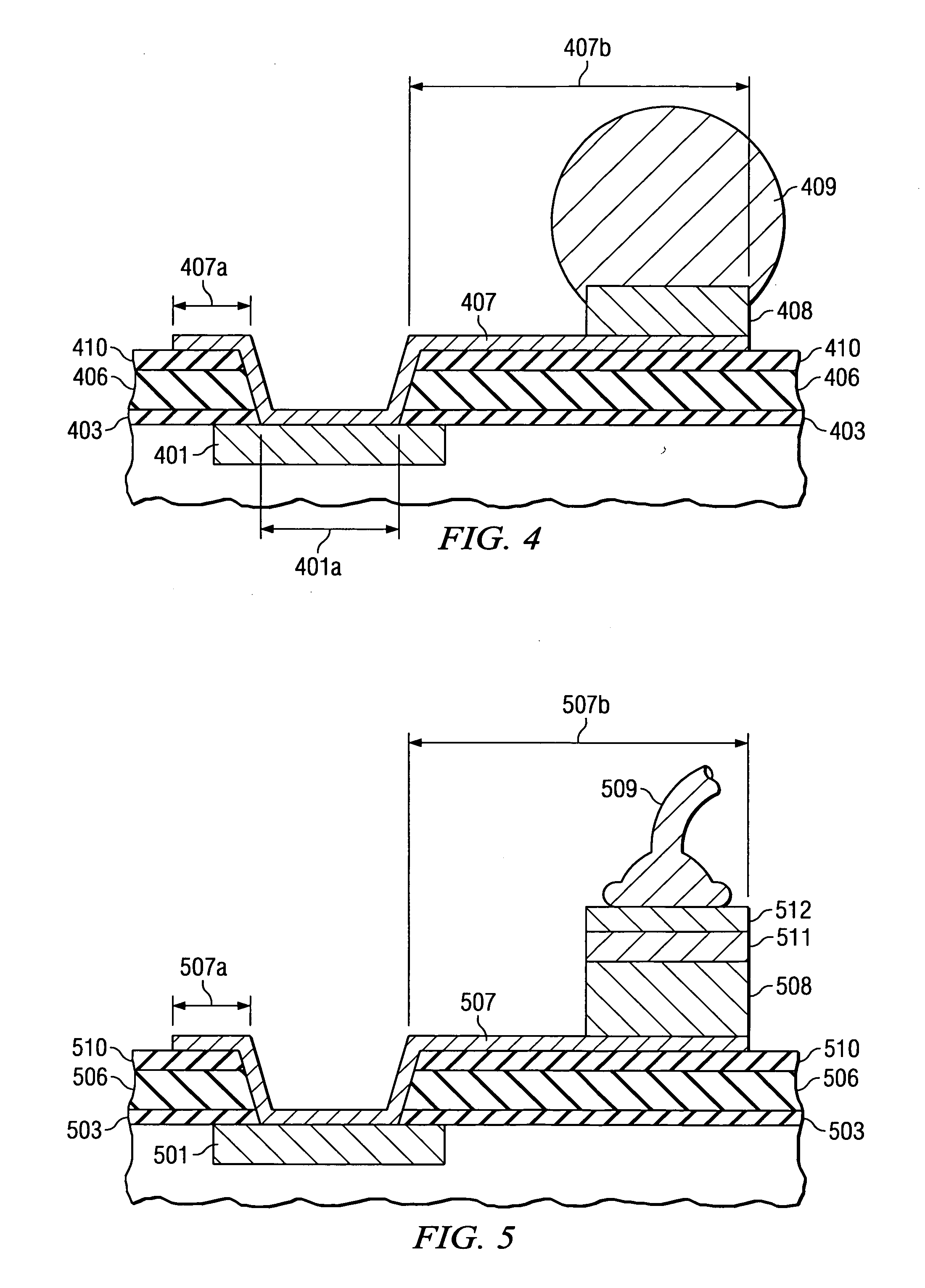
[0021] The impact of the present invention can be most easily appreciated by highlighting the shortcomings of the known approaches to form contacts to integrated circuits (ICs). FIG. 1 illustrates schematically an example of the metallurgical requirements in known technology for a contact pad of a small portion of an IC chip generally designated 100. A semiconductor material 101, typically silicon, has patterned aluminum metallization 102 and is protected by a dielectric, moisture-impermeable protective overcoat 103, usually silicon nitride or oxynitride. A window has been opened in the overcoat 103 to expose metallization 102 and leave a protective perimeter 103a around metallization 102. An additional “under bump” metallization 104 has been deposited onto metallization 102 and p...


PUM

PropertyMeasurementUnit
thicknessaaaaaaaaaa
thicknessaaaaaaaaaa
thickaaaaaaaaaa

Abstract

A semiconductor device including a contact pad and circuit metallization on the surface of an integrated circuit (IC) chip comprises a stack of protection layers over the surface of the chip. The stack consists of a first inorganic layer (303, preferably silicon nitride) on the chip surface, followed by a polymer layer (306, preferably benzocyclobutene) on the first inorganic layer (303), and finally an outermost second inorganic layer (310, preferably silicon dioxide) on the polymer layer (303). A window (301a) in the stack of layers exposes the metallization (301) of the IC. A patterned seed metal layer (307, preferably copper) is on the metallization (301) in the window and on the second inorganic layer (310) around the window. A buffer metal layer (308, preferably copper) is positioned on the seed metal layer (307). A metal reflow element (309) is attached to the buffer metal (308).

Description

FIELD OF THE INVENTION [0001] The present invention is related in general to the field of semiconductor devices and processes and more specifically to methods for sealing and protecting integrated circuit bonding pads to reduce the risk of delamination. DESCRIPTION OF THE RELATED ART [0002] When an integrated circuit (IC) chip is to be assembled on a substrate by the flip-chip technology, the connecting members between chip and substrate are typically shaped as balls or bumps, and are commonly made of reflowable metals such as solder. The chip metallization has most commonly been aluminum. For aluminum, it has been studied extensively in the semiconductor technology, how the chip contact pads have to be prepared to employ solder connections successfully. Because solder and the easily-oxidized aluminum cannot be contacted reliably, a major part of the pad preparation includes the deposition of so-called “under bump metals”. These metals form typically one or more layers over the cont...

Claims


Application Information

Patent Timeline
Patent Type & Authority Applications(United States)
IPC IPC(8): H01L23/31H01L23/485
CPCH01L23/3192H01L24/05H01L24/12H01L24/45H01L24/48H01L2224/0231H01L2224/04042H01L2224/05073H01L2224/05147H01L2224/05155H01L2224/05639H01L2224/05644H01L2224/05655H01L2224/05664H01L2224/05669H01L2224/13022H01L2224/13099H01L2224/45014H01L2224/45124H01L2224/45144H01L2224/45147H01L2224/48463H01L2224/4847H01L2924/01002H01L2924/01006H01L2924/01007H01L2924/01012H01L2924/01013H01L2924/01014H01L2924/01018H01L2924/01022H01L2924/01027H01L2924/01028H01L2924/01029H01L2924/0103H01L2924/01031H01L2924/01032H01L2924/01042H01L2924/01046H01L2924/01047H01L2924/01049H01L2924/0105H01L2924/01073H01L2924/01074H01L2924/01075H01L2924/01078H01L2924/01079H01L2924/01082H01L2924/01083H01L2924/014H01L2924/05042H01L2924/14H01L2924/3011H01L2924/01019H01L2924/01023H01L2924/01024H01L2924/01033H01L2924/01087H01L2224/05018H01L2224/05572H01L2224/48644H01L2224/48655H01L2224/48664H01L2224/48669H01L2224/48839H01L2224/48844H01L2224/48855H01L2224/48864H01L2224/48639H01L2224/48739H01L2224/48755H01L2224/48764H01L2224/48769H01L2924/10253H01L2224/0401H01L2924/0002H01L2924/00014H01L2924/00H01L2224/48869H01L2224/48744H01L2224/05552H01L2224/05556H01L2224/05568H01L2924/00012H01L2924/206
Inventor BOJKOV, CHRISTO P.TORRES, ORLANDO F.
Owner TEXAS INSTR INC
Why Eureka
Try Eureka