Circuitized substrate for fixing solder beads on pads

Active Publication Date: 2005-04-21
ADVANCED SEMICON ENG INC
View PDF8 Cites 13 Cited by
  • Summary
  • Abstract
  • Description
  • Claims
  • Application Information

AI Technical Summary

Benefits of technology

[0005] The primary object of the present invention is to provide a circuitized substrate having the capacity to control the location and the growth of solder beads. The paired contact pads on a substrate are expanded or diminished to form a plurality of bead receptacles at the facing corners thereof. When solder paste used for connecting a SMD is reflowed, the solder beads formed from solder paste can be fixed on the bead receptacles near the SMD. Therefore the circuitized substrate offers a better bonding strength for the SMD by fixing the solder beads for semiconductor packages.
[0007] According to the present invention, a circuitized substrate having paired contact pads for mounting a SMD, such as passive component selected from resistor, inductor, and capacitor. The SMD has a first terminal and a second terminal. The circuitized substrate mainly includes a substrate and a pair of contact pads. The paired contact pads are located on a surface of the substrate for connecting the first and second terminals of the SMD by means of reflowing solder paste. Each contact pad has at least a bead receptacle at the facing corner to fix solder beads formed from the reflowed solder paste. Therefore the bead receptacles can control the location of the solder beads and enhance the growth of the fixed solder beads on the corners of the contact pads.

Problems solved by technology

However, the substrate has a limited area for SMD's.
The solder paste will be pressed by the SMD and caused uncontrollably flow of solder paste on the contact pads during reflowing.
The solder beads will be free to move about on the substrate, resulting in severe contamination, moreover, electrical problems.
However, the solder beads are formed unpredictably due to the variation of the mounting pressure of SMD and the quantity of solder paste applied.
Once the solder beads are formed in the above-mentioned fin-shaped grooves, the solder beads cannot be easily bonded to the slender and acute-angled grooves which leads to short circuit.
Thus, it is not good to manufacture a semiconductor package using such a substrate as a chip carrier.
Besides, the solder mask with radial opening and metal contact pads are difficult to manufacture.

Method used


Image

  • Circuitized substrate for fixing solder beads on pads
  • Circuitized substrate for fixing solder beads on pads
  • Circuitized substrate for fixing solder beads on pads

Examples


first embodiment

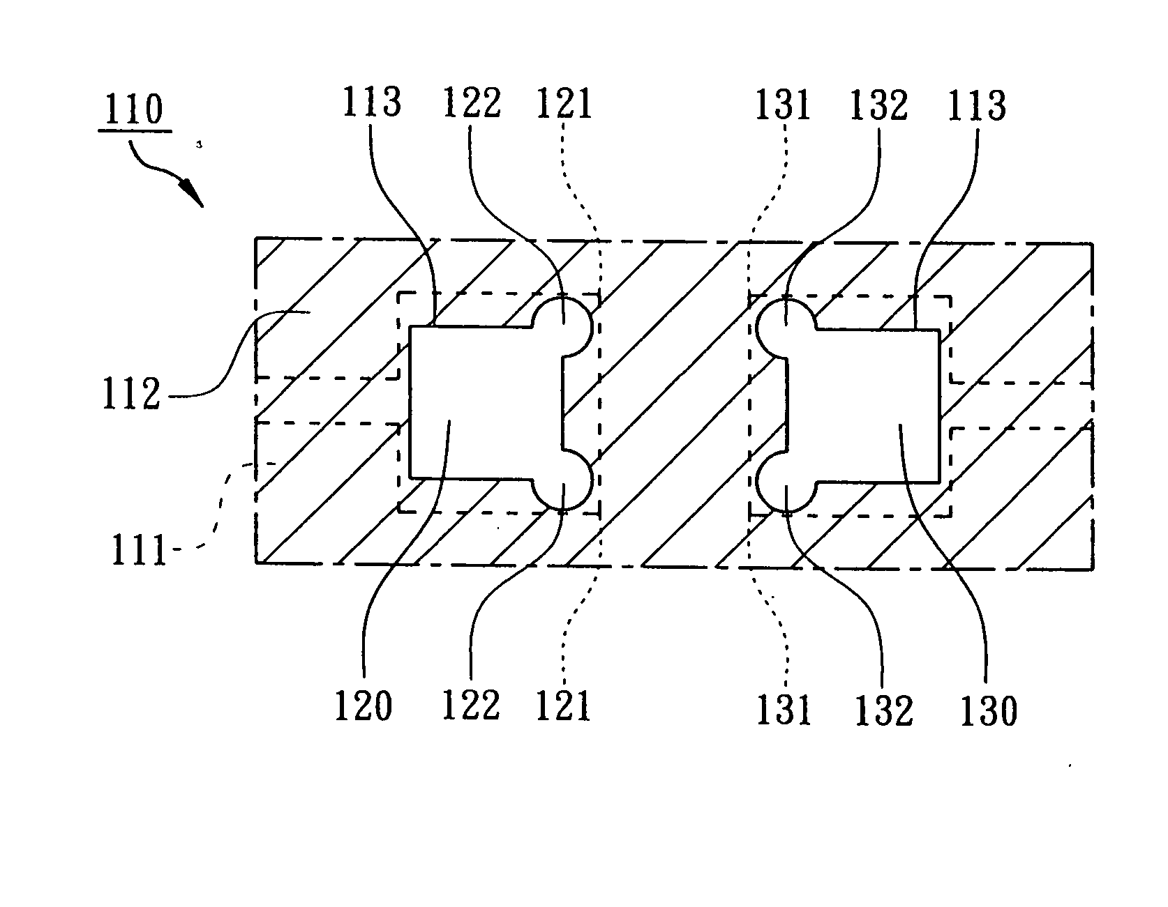
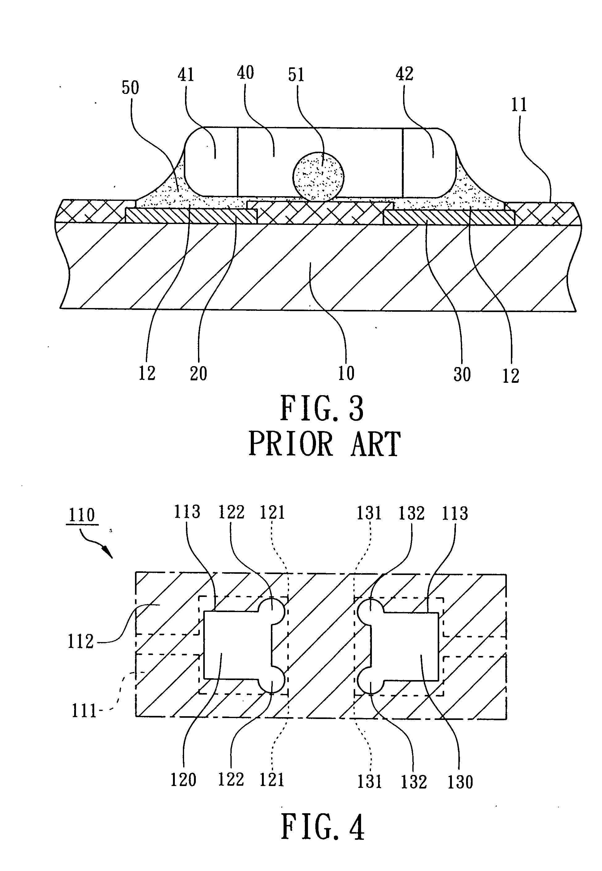
[0016] In the present invention, as shown in FIGS. 4, 5 and 6, a circuitized substrate is provided for fixing solder beads 151. The circuitized substrate has a plurality of paired contact pads for mounting a SMD 140 (surface mount device), a first contact pad 120 and a corresponding contact pad 130 are illustrated in this embodiment. The SMD 140 may be a passive component selected from the group consisting of resistor, inductor, or capacitor. Referring to FIGS. 5 and 6 again, the SMD 140 has a first terminal 141 and a second terminal 142. The circuitized substrate includes a substrate 110, a first contact pad 120, and a second contact pad 130. Preferably, the circuitized substrate is a chip carrier for semiconductor packages, which has at least a layer of wiring pattern, such as a printed circuit board, a ceramic circuit board, a wiring film, a semiconductor substrate, or even a wafer. The substrate 110 has a surface 111 as component-mounted surface. The first contact pad 120 and th...

second embodiment

[0020] In second embodiment, a circuitized substrate is illustrated as shown in FIG. 7. A first contact pad 220 and a second contact pad 230 are located on a substrate 210 respectively and are expanded to form a plurality of bead receptacles 221 and 231 at the facing corners thereof. A solder mask 211 is formed on the substrate 210. In this embodiment, the openings 212 of the solder mask 211 are larger than the first contact pad 220 and the second contact pad 230 to completely expose the first contact pad 220, the second contact pad 230 and the bead receptacles 221, 231. Thus, the first contact pad 220 and the second contact pad 230 are Non-Solder-Mask Defined pads (NSMD pad) with the capability of fixing the solder beads. The location of the fixed solder beads can be expected and the growth of the fixed solder beads can be enhanced helpful for semiconductor packages.


PUM

PropertyMeasurementUnit
Diameteraaaaaaaaaa

Abstract

A circuitized substrate has contact pads for mounting a Surface Mount Device (SMD). First and second contact pads are located on a surface of the substrate corresponding to a first terminal and a second terminal of the SMD. The first and the second contact pads have a plurality of expanded portion or diminished portions to form bead receptacles at the facing corners thereof. When solder paste is reflowed to electrically connect the SMD, solder beads formed from the solder paste can be fixed on the bead receptacles. Therefore, there is no free solder bead on the substrate causing short circuit for semiconductor packages.

Description

FIELD OF THE INVENTION [0001] The present invention generally relates to a circuitized substrate for mounting a SMD (Surface Mount Device), more particularly to a circuitized substrate having improved contact pads for fixing the solder beads for semiconductor packages. BACKGROUND OF THE INVENTION [0002] SMD (Surface Mount Device), such as passive components selected from resistors, inductors or capacitors, are mounted on the contact pads of a circuitized substrate like printed circuit board or ceramic substrate. Recently, more and more components and SMD's are requested to mount on a chip-carrying substrate especially for Multi-Chip Package / Module, Chip Scale Package, or System-In-Package. However, the substrate has a limited area for SMD's. Generally, solder paste serves as an electrical connection agent for mounting SMD on the contact pads of a substrate. The solder paste will be pressed by the SMD and caused uncontrollably flow of solder paste on the contact pads during reflowing...

Claims


Application Information

Patent Timeline
IPC IPC(8): B23K3/06B23K31/02H01L23/13H05K1/11H05K3/34
CPCB23K3/06B23K2201/42H05K1/111H05K2201/10636H05K3/3452H05K2201/09381H05K2201/099H05K3/3442B23K2101/42Y02P70/50
Inventor LIU, SHENG-TSUNG
Owner ADVANCED SEMICON ENG INC
Why Eureka
Try Eureka