Light emitting device
a technology of light emitting device and light emitting tube, which is applied in the direction of static indicating device, discharge tube luminescnet screen, instruments, etc., can solve the problems of poor formation of el layer, and achieve the effect of reducing consumption of electric power and high definition
- Summary
- Abstract
- Description
- Claims
- Application Information
AI Technical Summary
Benefits of technology
Problems solved by technology
Method used
Image

Examples
embodiment 1
[Embodiment 1]
[0086] Here, a method of simultaneously manufacturing TFTs (n-channel TFT and p-channel TFT) in a pixel portion and a driver circuit provided in the periphery of the pixel portion on the same substrate and manufacturing an EL element are described in detail with reference to FIGS. 3A to 6.
[0087] First, in this embodiment, a substrate 300 is used, which is made of glass such as barium borosilicate glass or alumino borosilicate glass, typified by #7059 glass or #1737 glass of Corning Inc. There is no limitation on the substrate 300 as long as a substrate having a light transmitting property is used, and a quartz substrate may also be used. In addition, a plastic substrate having heat resistance to a treatment temperature of this embodiment may also be used.
[0088] Then, a base film 301 formed of an insulating film such as a silicon oxide film, a silicon nitride film or a silicon oxide nitride film is formed on the substrate 300. In this embodiment, a two-layer structure...
embodiment 2
[Embodiment 2]
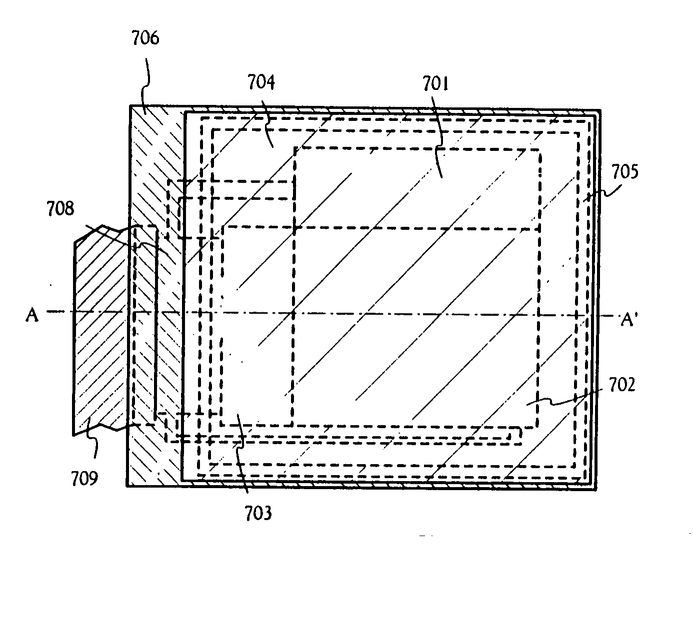
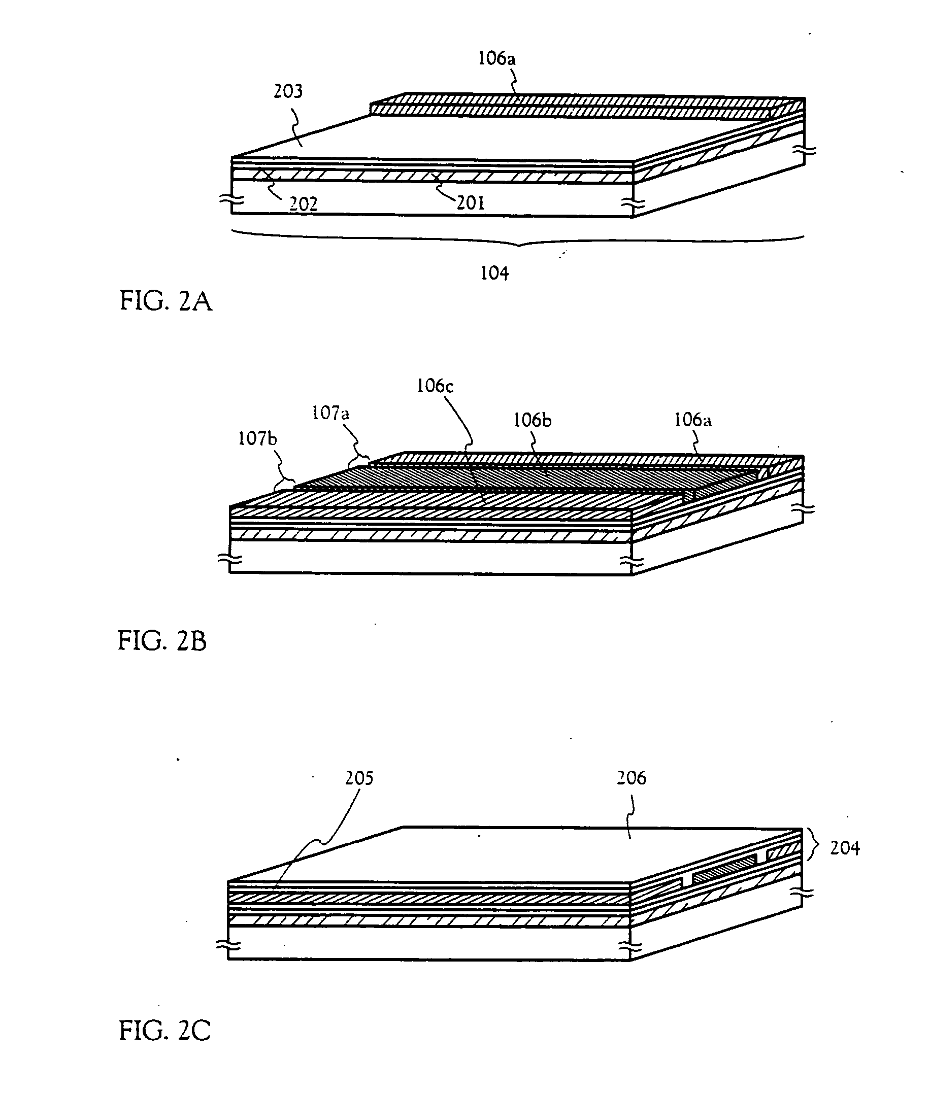
[0147] In this embodiment, a method of completing the EL module shown in FIG. 6 as a light emitting device is described with reference to FIGS. 7A and 7B.
[0148]FIG. 7A is a top surface diagram showing a state completed up through sealing of an EL element. FIG. 7B is a cross sectional view taken along a line A-A′ of FIG. 7A. Reference numeral 701 indicated by a dotted line indicates a source side driver circuit, reference numeral 702 indicates a pixel portion, and reference numeral 703 indicates a gate side driver circuit. Further, reference numeral 704 indicates a cover member, reference numeral 705 indicates a first sealant, and reference numeral 706 indicates a second sealant. The inside surrounded by the first sealant 705 is a space.
[0149] Note that reference numeral 708 indicates a wiring for transmitting a signal input to the source side driver circuit 701 and the gate side driver circuit 703, and the wiring receives a video signal or a clock signal from an FPC ...
embodiment 3
[Embodiment 3]
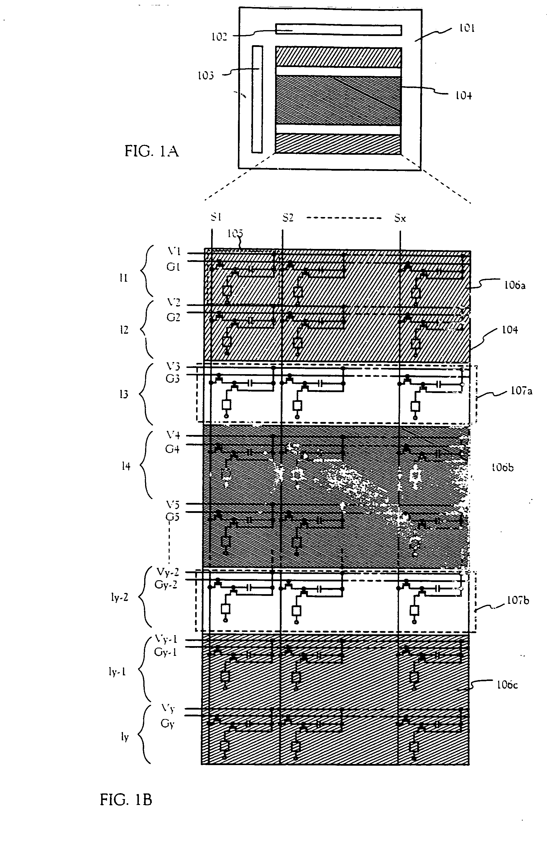
[0158] A detailed top surface structure of a pixel portion is shown in FIG. 8A, and a circuit diagram thereof is shown in FIG. 8B. In FIGS. 8A and 8B, a switching TFT 804 provided on a substrate is formed by using the switching TFT (n-channel type) TFT 503 of FIG. 6. Therefore, an explanation of the switching (n-channel type) TFT 503 may be referred for an explanation of the structure. Further, a wiring indicated by reference numeral 803 is a gate wiring for electrically connecting with gate electrodes 804a and 804b of the switching TFT 804.
[0159] Note that, in this embodiment, a double gate structure is adopted, in which two channel forming regions are formed, but a single gate structure, in which one channel forming region is formed, or a triple gate structure, in which three channel forming regions are formed, may also be adopted.
[0160] Further, a source of the switching TFT 804 is connected to a source wiring 815, and a drain thereof is connected to a drain wirin...
PUM
 Abstract
Description
Claims
Application Information
 - Generate Ideas
- Intellectual Property
- Life Sciences
- Materials
- Tech Scout
- Unparalleled Data Quality
- Higher Quality Content
- 60% Fewer Hallucinations
Browse by: Latest US Patents, China's latest patents, Technical Efficacy Thesaurus, Application Domain, Technology Topic, Popular Technical Reports.
© 2025 PatSnap. All rights reserved.Legal|Privacy policy|Modern Slavery Act Transparency Statement|Sitemap|About US| Contact US: help@patsnap.com