Method for fabricating a silicon nanocrystal, silicon nanocrystal, method for fabricating a floating gate type memory capacitor structure, and floating gate type memory capacitor structure

a technology of memory capacitor and nanocrystal, which is applied in the field of a method for fabricating a floating gate type memory capacitor structure, can solve the problems of large fluctuation of nanocrystal, inability to meet the above-mentioned requirement, and inability to assemble nanocrystals by the combination method, etc., to achieve the effect of easy formation

Inactive Publication Date: 2005-04-28
NAGOYA UNIVERSITY
View PDF13 Cites 4 Cited by
  • Summary
  • Abstract
  • Description
  • Claims
  • Application Information

AI Technical Summary

Benefits of technology

[0010] In the present invention, an amorphous silicon layer with a minute thickness is formed on a silicon substrate, and then, a raw material gas is supplied onto the amorphous silicon layer to form a silicon nanocrystal. In this case, the amorphous silicon layer functions satisfactorily as a nucleus for the growth of the high density and minute silicon nanocrystal. As a result, the silicon nanocrystal can be rendered high density and minute so that the number density of the silicon nanocrystal can be developed to 1×10¹² / cm2 and the crystal grain size of the silicon nanocrystal can be micronized to 10 nm or below. Therefore, the silicon nanocrystal can be employed as a dot memory, and thus, a semiconductor dot memory made of the silicon nanocrystal can be provided.
[0012] In a preferred embodiment of the present invention, the thickness of the amorphous silicon layer is set to 1 nm or below. In this case, the high density and minute silicon nanocrystal can be made easily.
[0013] In the formation of the silicon nanocrystal, advantageously, the silicon substrate is heated within a temperature range of 200-1000° C., preferably within a temperature range of 400-800° C. In this case, only if the amorphous silicon layer is exposed to the raw material gas, the silicon nanocrystal can be formed. That is, the silicon nanocrystal can be formed easily.

Problems solved by technology

However, the nanocrystal to satisfy the above-mentioned requirement has not been fabricated by the combination method.
With the repeated method, however, the adjacent nanocrystal dots are overlapped so that the arrangement density of the nanocrystal dots can not be uniform and the performance of the semiconductor dot memory using the nanocrystal fluctuated largely.

Method used


Image

  • Method for fabricating a silicon nanocrystal, silicon nanocrystal, method for fabricating a floating gate type memory capacitor structure, and floating gate type memory capacitor structure
  • Method for fabricating a silicon nanocrystal, silicon nanocrystal, method for fabricating a floating gate type memory capacitor structure, and floating gate type memory capacitor structure
  • Method for fabricating a silicon nanocrystal, silicon nanocrystal, method for fabricating a floating gate type memory capacitor structure, and floating gate type memory capacitor structure

Examples


example 1

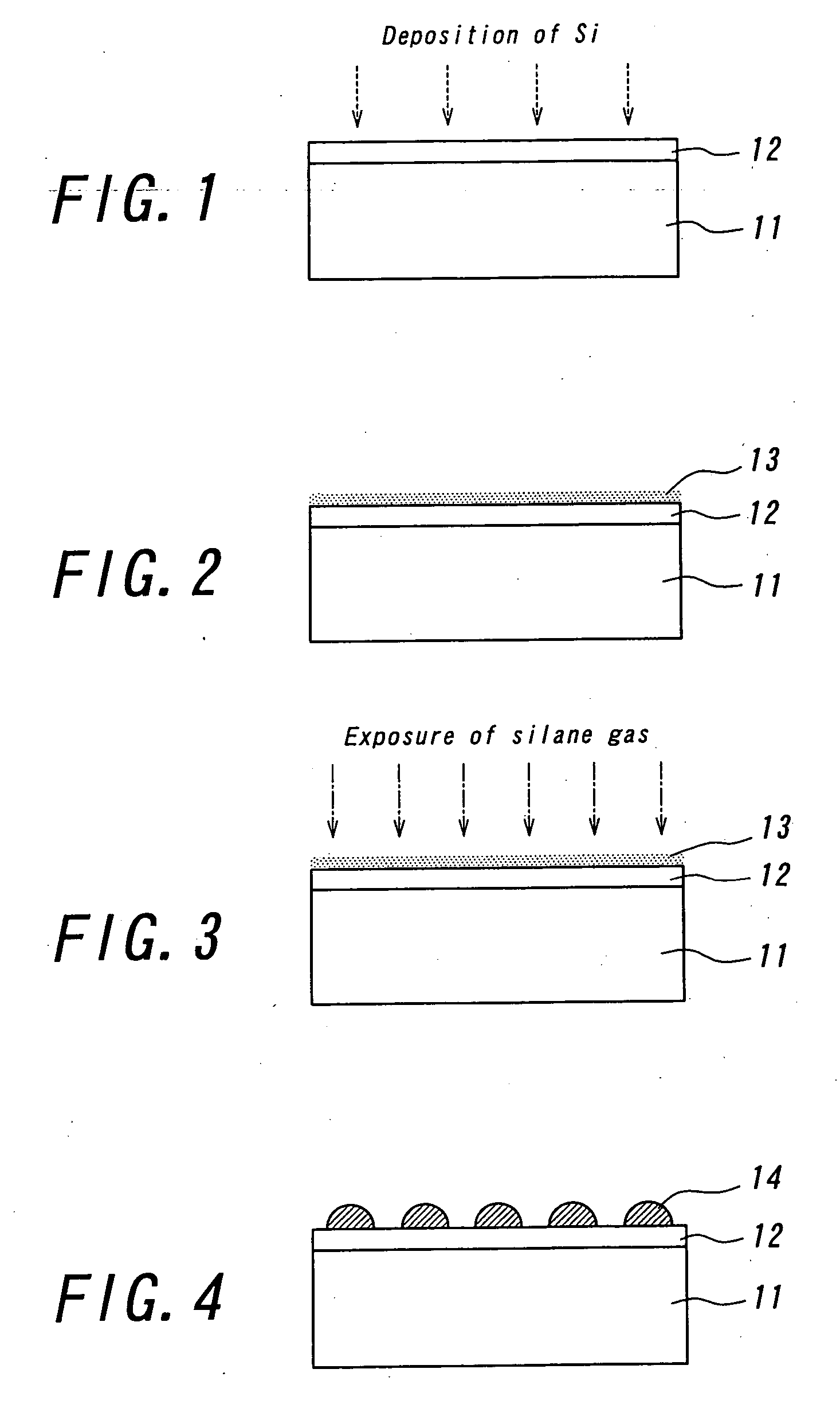
[0046] The thickness of the amorphous silicon layer 13 was set to 1 nm, and the silicon substrate 11 was heated to 610° C. Then, a disilane gas (Si2H6) was employed as a raw material gas to form the silicon nanocrystal 14 according to the steps illustrated in FIGS. 1-4. FIG. 9 is a high resolution TEM photograph of the silicon nanocrystal 14. It was turned out from FIG. 9 that the crystal grain size of the silicon nanocrystal 14 was about 10 nm. Moreover, it was confirmed from the TEM observation that the arrange density and the crystal grain size of the silicon nanocrystal 14 was almost uniform.

example 2

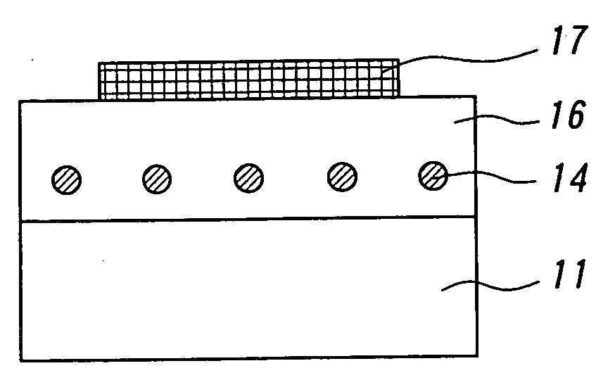
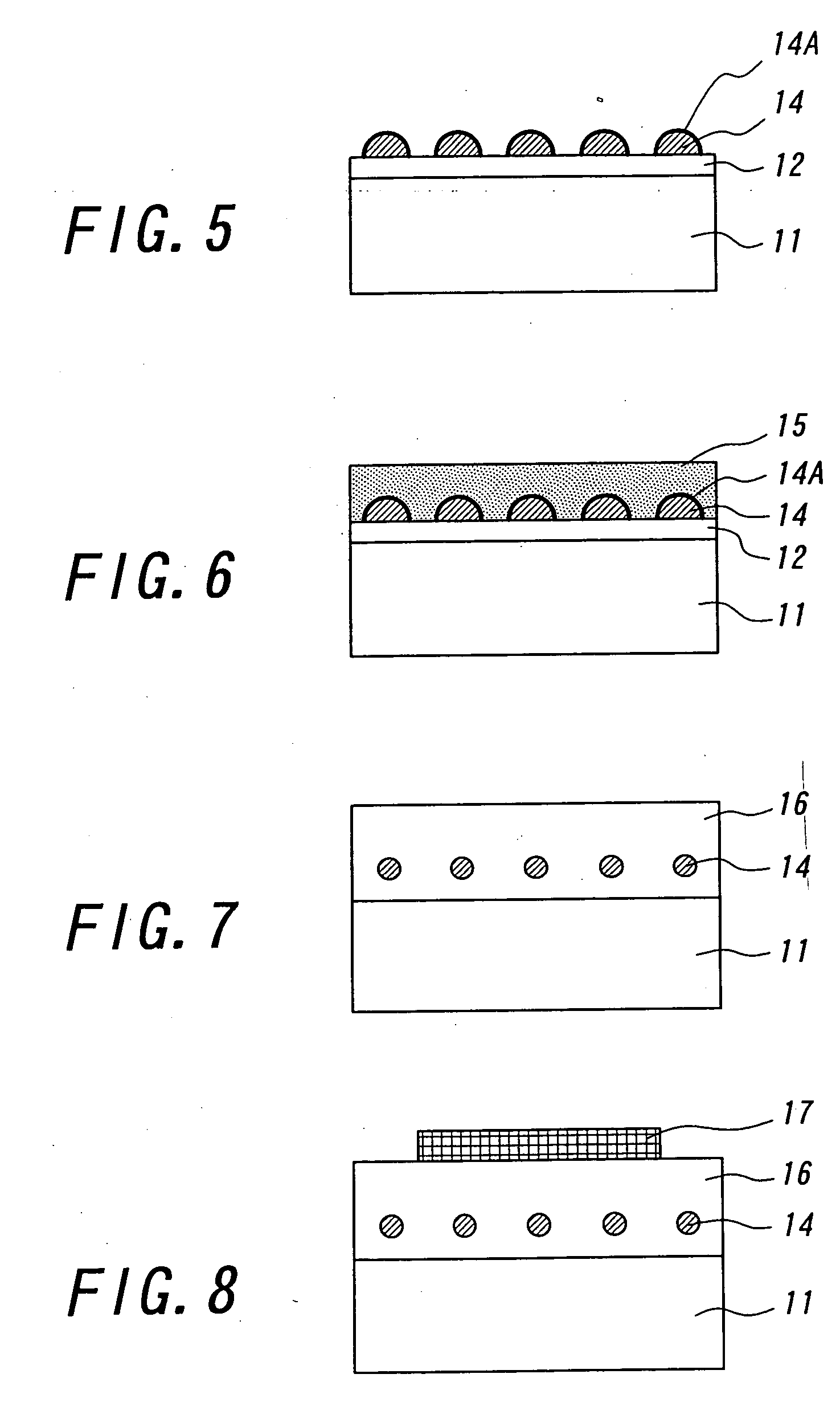
[0047] The steps illustrated in FIGS. 5-7 were carried out for the silicon nanocrystal 14 obtained in Example 1. The thickness of the additional amorphous silicon layer 15 was set to 20 nm. FIG. 10 is also a high resolution TEM photograph of the silicon nanocrystal 14. It was turned out from FIG. 10 that the crystal grain size of the silicon nanocrystal 14 was narrowed to 5 nm through the thermal oxidizing treatment as mentioned above. Moreover, it was confirmed from the TEM observation that the arrange density and the crystal grain size of the narrowed silicon nanocrystal 14 was almost uniform.


PUM

PropertyMeasurementUnit
thicknessaaaaaaaaaa
temperatureaaaaaaaaaa
crystal grain sizeaaaaaaaaaa

Abstract

A silicon oxide layer is formed at a surface region of a silicon substrate. Then, an amorphous silicon layer 13 is formed preferably in a thickness of 1 nm or below on the silicon substrate via the silicon oxide layer. Then, the amorphous silicon layer 13 is exposed to a silane gas preferably with heating the silicon substrate within a temperature range of 400-800° C. to form a high density and minute silicon nanocrystal.

Description

BACKGROUND OF THE INVENTION [0001] 1. Field of the Invention [0002] This invention relates to a method for fabricating a silicon nanocrystal, a silicon nanocrystal, a method for fabricating a floating gate type memory capacitor structure, and a floating gate type memory capacitor structure. [0003] 2. Description of the Related Art [0004] In semiconductor dot memory field is required a high density nanocrystal with a number density of 1×10¹² / cm2 or over and a crystal grain size of 10 nm or below. In the fabrication of the nanocrystal, conventionally, the combination of a conventional film forming technique with a surface chemical treatment (chemical solution treatment) has been employed. However, the nanocrystal to satisfy the above-mentioned requirement has not been fabricated by the combination method. [0005] In this point of view, such an attempt is made as to repeat the combination method several times to form the intended nanocrystal at multistage. With the repeated method, howe...

Claims


Application Information

Patent Timeline
Patent Type & Authority Applications(United States)
IPC IPC(8): C01B33/027C30B1/00H01L21/02H01L21/20H01L21/205H01L21/28H01L21/336H01L21/8242H01L21/8247H01L27/115H01L29/423H01L29/76H01L29/788H01L29/792
CPCB82Y10/00H01L21/28273H01L29/42332H01L21/0262H01L21/02488H01L21/02532H01L21/02601H01L21/02381H01L29/40114
Inventor KONDO, HIROKIYASUDA, YUKIOZAIMA, SHIGEAKISAKAI, AKIRASAKASHITA, MITSUONAITO, SHINYASATAKE, MASAKI
Owner NAGOYA UNIVERSITY
Why Eureka
Try Eureka