Optical signal transmission apparatus including reflective gain-clamped semiconductor optical amplifier

a semiconductor optical amplifier and optical signal transmission technology, applied in the direction of semiconductor amplifier structure, multiplex communication, semiconductor lasers, etc., can solve the problems of inability to effectively implement wdm-pon, heavy economic burden on subscribers, and complicated manufacturing processes of dfb laser arrays and mfls, so as to effectively suppress the intensity noise of an incoherent light source and improve modulation speed and optical power

Inactive Publication Date: 2005-04-28
SAMSUNG ELECTRONICS CO LTD
View PDF9 Cites 50 Cited by
  • Summary
  • Abstract
  • Description
  • Claims
  • Application Information

AI Technical Summary

Benefits of technology

[0015] Accordingly, the present invention has been made to reduce or overcome the above-mentioned problems occurring in the prior art. One object of the present invention is to provide an optical signal transmission apparatus including a reflective gai

Problems solved by technology

However, in spite of these advantages, the WDM-PON has not yet been put to practical use.
This, in turn, places a heavy economic burden on subscribers.
However, the DFB laser array and the MFL have complicated manufacturing processes.
However, they have narrow modulation bandwidths and low output power.
However, it has a narrow bandwidth, thus cannot provide a number of wavelength-divided channels.
Also, with the FP laser, serious degradation is caused by mode parti

Method used


Image

  • Optical signal transmission apparatus including reflective gain-clamped semiconductor optical amplifier
  • Optical signal transmission apparatus including reflective gain-clamped semiconductor optical amplifier
  • Optical signal transmission apparatus including reflective gain-clamped semiconductor optical amplifier

Examples


Embodiment Construction

[0028] Hereinafter, the present invention will be described with reference to the accompanying drawings. For the purposes of clarity and simplicity, a detailed description of known functions and configuration incorporated herein will be omitted as it may make the subject matter of the present invention unclear.

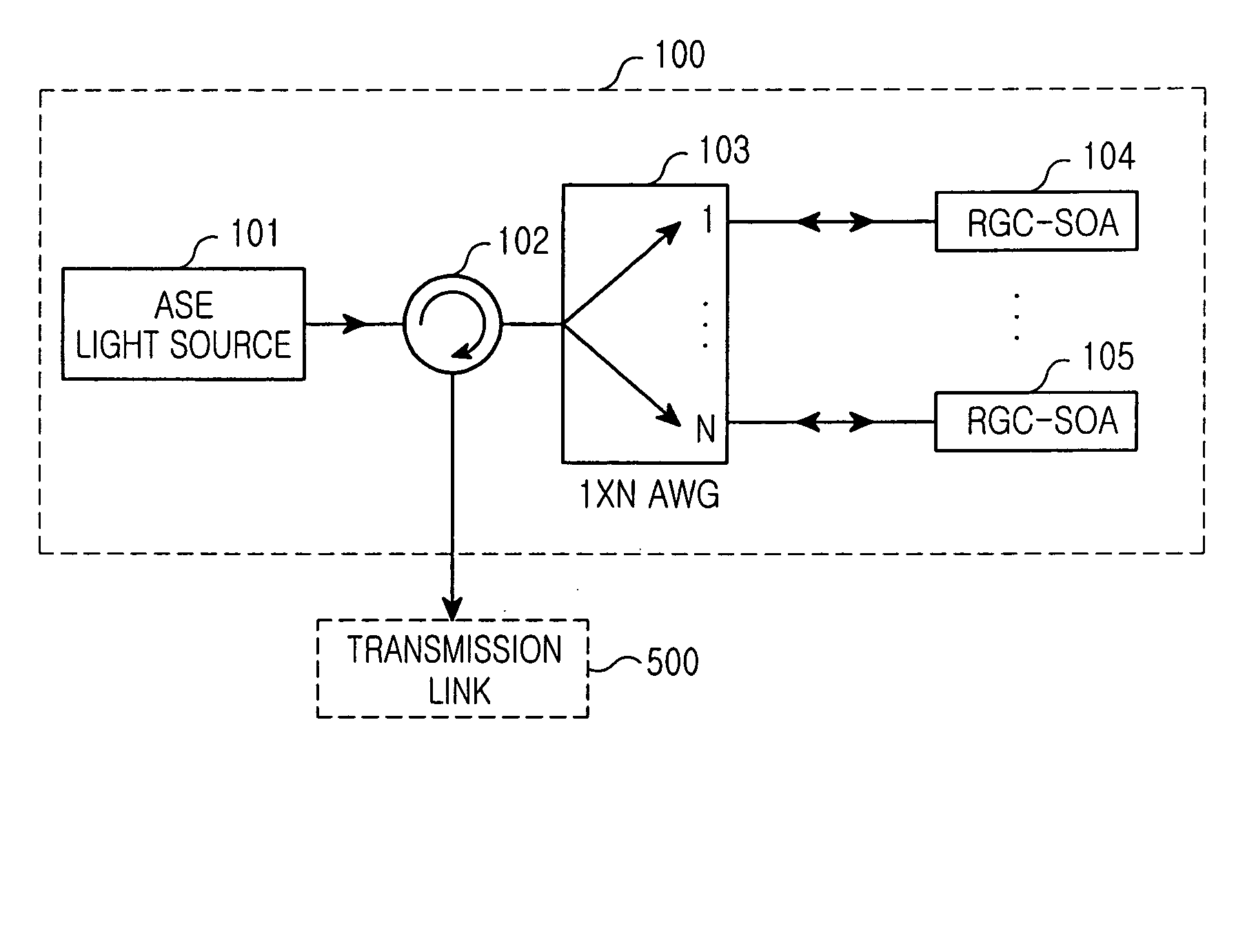
[0029]FIG. 1 is a block diagram of an optical signal transmission apparatus using a gain-clamped semiconductor optical amplifier according to a preferred embodiment of the present invention. The optical signal transmission apparatus 100 of the present invention outputs wavelength division multiplexed optical signals to an optical transmission link 500. The apparatus 100 includes an amplified spontaneous emission source (hereinafter, referred to as an ASE source) 101, an optical circulator 102, a 1×N arrayed waveguide grating (AWG) 103, and a number N of reflective gain-clamped semiconductor optical amplifiers 104 to 105.

[0030] The ASE source 101 has a wide wavelength band, w...


PUM


Abstract

Disclosed are optical signal transmission apparatus including a reflective gain-clamped semiconductor optical amplifier and optical communication system using the optical signal transmission apparatus, which can improve modulation speed and optical power by effectively suppressing intensity noise of an incoherent light source. The optical signal transmission apparatus comprises a light source; a reflective gain-clamped semiconductor optical amplifier to generate gain-clamped optical signals having a substantially constant output intensity in a gain saturation region; a wavelength division multiplexing apparatus configured to spectrum-slice light from the light source, provide the spectrum-sliced light to the reflective gain-clamped semiconductor optical amplifier, and multiplex optical signals gain-clamped by the reflective gain-clamped optical amplifier. and a circulator for inputting the light generated by the light source to the wavelength division multiplexing apparatus, and outputting the optical signal multiplexed by the wavelength division multiplexing apparatus to a transmission link.

Description

CLAIM OF PRIORITY [0001] This application claims priority to an application entitled “Optical signal transmission apparatus including reflective gain-clamped semiconductor optical amplifier and optical communication system using the same,” filed in the Korean Intellectual Property Office on Oct. 27, 2003 and assigned Serial No. 2003-75193, the contents of which are hereby incorporated by reference. BACKGROUND OF THE INVENTION [0002] 1. Field of the Invention [0003] The present invention relates to wavelength division multiplexing optical communication, and more particularly to an optical signal transmission apparatus including a reflective gain-clamped semiconductor optical amplifier and an optical communication system using the optical signal transmission apparatus. [0004] 2. Description of the Related Art [0005] Generally, a wavelength division multiplexing passive optical network (hereinafter, referred to as a WDM PON) provides an ultra high-speed broadband communication service ...

Claims


Application Information

Patent Timeline
IPC IPC(8): G02B6/28H01S5/50H01S3/00H01S3/23H01S5/00H04B10/2507H04B10/40H04B10/50H04B10/60H04J14/00H04J14/02
CPCH01S3/2333H01S3/2383H01S2301/02H01S5/5072H04B10/506H01S5/005G02B6/28
Inventor LEE, JEONG-SEOKKIM, HO-INYUN, IN-KUKKIM, SEUNG-WOOSHIN, HYUN-CHEOLOH, YUN-JEHWANG, SEONG-TAEK
Owner SAMSUNG ELECTRONICS CO LTD
Why Eureka
Try Eureka